CMOS image sensor and method for fabricating the same

Inactive Publication Date: 2006-05-11
DONGBU ELECTRONICS CO LTD
View PDF6 Cites 14 Cited by
  • Summary
  • Abstract
  • Description
  • Claims
  • Application Information

AI Technical Summary

Benefits of technology

[0015] An advantage of the present invention is to provide a CMOS image sensor and a method for fabricating the same, which enhances the light-receiving capability of an image sensor by configuring a microlens to comprise central and peripheral parts. Each of the central and peripheral parts are imparted with a predetermined convex curvature to maximize light transmitted to an active device for generating an electrical charge according to the intensity of an incoming light signal.
[0016] Additional features and advantages of the invention will be set forth in the description which follows, and in part will be apparent from the description, or may be learned by practice of the invention. The objectives and other advantages of the invention will be realized and attained by the structure and method particularly pointed out in the written description and claims hereof as well as the appended drawings.
[0017] To achieve these and other advantages and in accordance with the purpose of the present invention, as embodied and broadly described, there is provided a CMOS image sensor comprising at least one microlens formed by anisotropic etching to have a focusing centerline, a central lens portion, and a peripheral lens portion, wherein the focusing centerline passes through the central lens portion and wherein the peripheral lens portion surrounds the central lens portion.
[

Problems solved by technology

Disadvantages of a general charge-coupled device include a complicated driving method, high power consumption, and a complicated fabrication process requiring a multi-phased photo process.
In a charge-coupled device, integration of complementary circuitry such as a control circuit,

Method used


Image

  • CMOS image sensor and method for fabricating the same
  • CMOS image sensor and method for fabricating the same
  • CMOS image sensor and method for fabricating the same

Examples


Embodiment Construction

[0027] Reference will now be made in detail to embodiments of the present invention, examples of which are illustrated in the accompanying drawings. Wherever possible, like reference designations will be used throughout the drawings to refer to the same or similar parts.

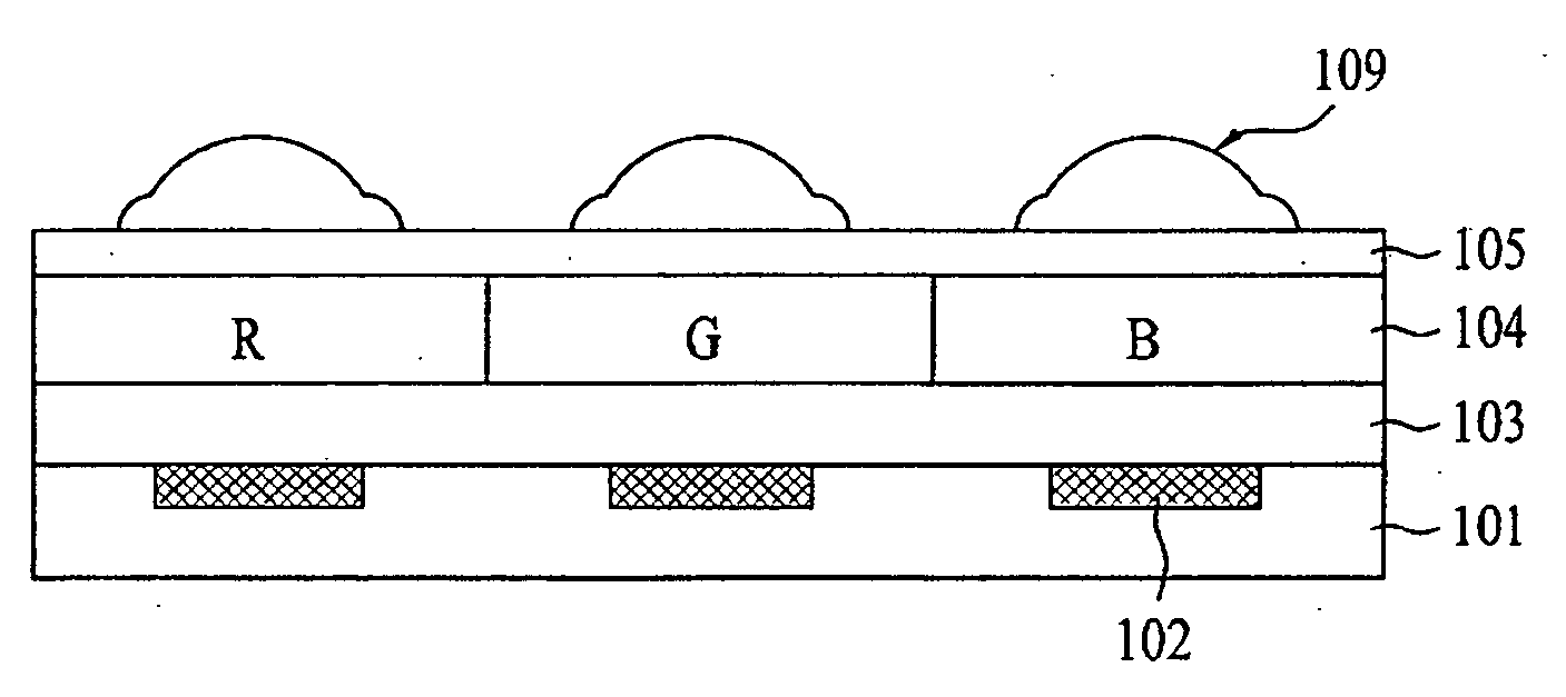
[0028] Referring to FIG. 6A, an insulating interlayer 103 is formed on a semiconductor substrate 101 having at least one photodiode 102 formed in a predetermined surface of the semiconductor substrate. Each photodiode is configured with various transistors (not shown) and a unit pixel of the CMOS image sensor is formed. Photodiodes 102 are active devices for generating an electrical charge according to the intensity of an incoming light signal and may be a photo-gate type device. The insulating interlayer 103 may include an optical shielding layer (not shown) to prevent light from entering a substrate area other than at one of the photodiodes 102. A color filter layer 104, comprised of an array of red (R), green (G)...


PUM


Abstract

A CMOS image sensor and fabricating method thereof enhances a light-receiving capability of an image sensor by preventing poor light-refraction characteristics at the peripheral part of a microlens. The CMOS image sensor includes at least one microlens formed by anistropic etching to have a focusing centerline, a central lens portion, and a peripheral lens portion, wherein the focusing centerline passes through the central lens portion and wherein the peripheral lens portion surrounds the central lens portion. The central lens portion has a first convex curvature based on a first radius and the peripheral lens portion has second convex curvature based on a second radius, wherein the second radius is greater than the first radius.

Description

This application claims the benefit of Korean Patent Application No. 10-2004-0090796, filed on Nov. 9, 2004, which is hereby incorporated by reference for all purposes as if fully set forth herein. BACKGROUND OF THE INVENTION [0001] 1. Field of the Invention [0002] The present invention relates to a CMOS image sensor and a method for fabricating the same. The present invention is suitable for a wide scope of applications, and is particularly suitable for enhancing a light-receiving capability of the image sensor. [0003] 2. Discussion of the Related Art [0004] Image sensors are semiconductor devices for converting an optical image into an electrical signal and include charge-coupled devices and complementary metal-oxide-semiconductor (CMOS) image sensors. A general charge-coupled device includes an array of photodiodes that convert light signals into electrical signals. Disadvantages of a general charge-coupled device include a complicated driving method, high power consumption, and ...

Claims


Application Information

Patent Timeline
IPC IPC(8): H01L31/113H01L31/062
CPCH01L27/14609H01L27/14621H01L27/14627H01L27/14643H01L27/14685H01L27/146H01L31/10
Inventor LEE, KAE HOON
Owner DONGBU ELECTRONICS CO LTD
Why Eureka
Try Eureka