Flexible wiring substrate, semiconductor device and electronic device using flexible wiring substrate, and fabricating method of flexible wiring substrate

a technology of flexible wiring and wiring substrate, which is applied in the direction of printed circuit aspects, sustainable manufacturing/processing, final product manufacturing, etc., can solve the problems of difficult to realize in the actual tcp such a fine pitch of wiring pattern, difficult to form a wiring pattern having a pitch of less than 45 m, etc., to achieve good shape, improve mechanical strength of wiring pattern, reduce variation in thickness of wiring pattern (inner lead).

Active Publication Date: 2006-05-11
SHENZHEN TOREY MICROELECTRONIC TECH CO LTD
View PDF8 Cites 22 Cited by
  • Summary
  • Abstract
  • Description
  • Claims
  • Application Information

AI Technical Summary

Benefits of technology

[0025] The present invention was made to solve the foregoing problems. An object of the present invention is to provide (i) a flexible wiring substrate having a structure: in which a wiring pattern is designed with a fine pitch and formed by etching so as to have a good shape; in which a variation in thickness of the wiring pattern (inner lead) is reduced; and in which mechanical strength of the wiring pattern is improved so as to prevent brakes or exfoliation of the wiring pattern, (ii) a semiconductor device and an electronic device which use the flexible wiring substrate, and (iii) a fabricating method of the flexible wiring substrate.

Problems solved by technology

As such, it is difficult to form a wiring pattern having a pitch of below 45 μm.
As described here, it is difficult to realize in the actual TCP such a fine pitch of the wiring pattern.
For example, one of the above problems is that, when realizing a fine pitch of a wiring pattern (inner lead), it becomes difficult to carry out a pattern etching with respect to the wiring pattern (inner lead) so that the wiring pattern has a good shape while the wiring pattern has a conventional thickness of 8 μm.
This makes it difficult that the wiring pattern is etched so as to have a good trapezoid cross section.
However, with a wiring pitch of less than 35 μm, it becomes difficult to carry out an etching process to have a trapezoid cross section which indicates a good cross sectional shape of the wiring pattern 105.
However, the reduction in thickness of the wiring pattern (inner lead), caused by realization of fine pitch of the wiring pattern, gives rise to the problem of degrading the mechanical strength of the wiring pattern.
This may cause the wiring pattern to be broken or exfoliated during a period: from a step for connecting and mounting a semiconductor element to a step for mounting a module of a COF semiconductor device.
However, due to the degrading of its mechanical strength, the wiring pattern may tend to be broken or exfoliated during a period from the step for connecting and mounting a semiconductor element to the step for mounting a module of a COF semiconductor device.
However, the conventional techniques do not easily enable realization of fine pitch design as described above, because the COF needs to be flexibly folded while requiring improved mechanical strength which allows reduction in thickness of the wiring pattern.

Method used


Image

  • Flexible wiring substrate, semiconductor device and electronic device using flexible wiring substrate, and fabricating method of flexible wiring substrate
  • Flexible wiring substrate, semiconductor device and electronic device using flexible wiring substrate, and fabricating method of flexible wiring substrate
  • Flexible wiring substrate, semiconductor device and electronic device using flexible wiring substrate, and fabricating method of flexible wiring substrate

Examples


first embodiment

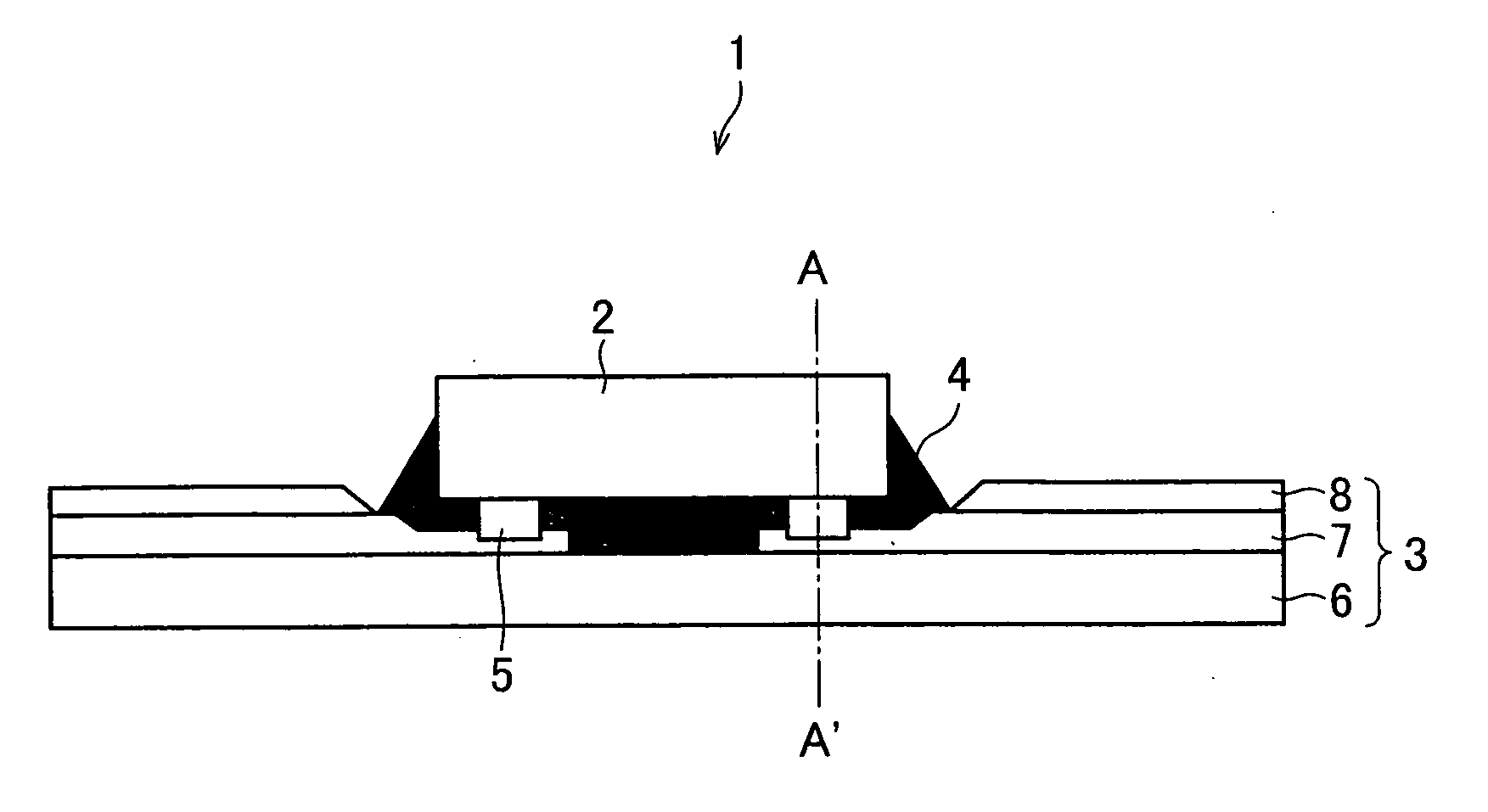
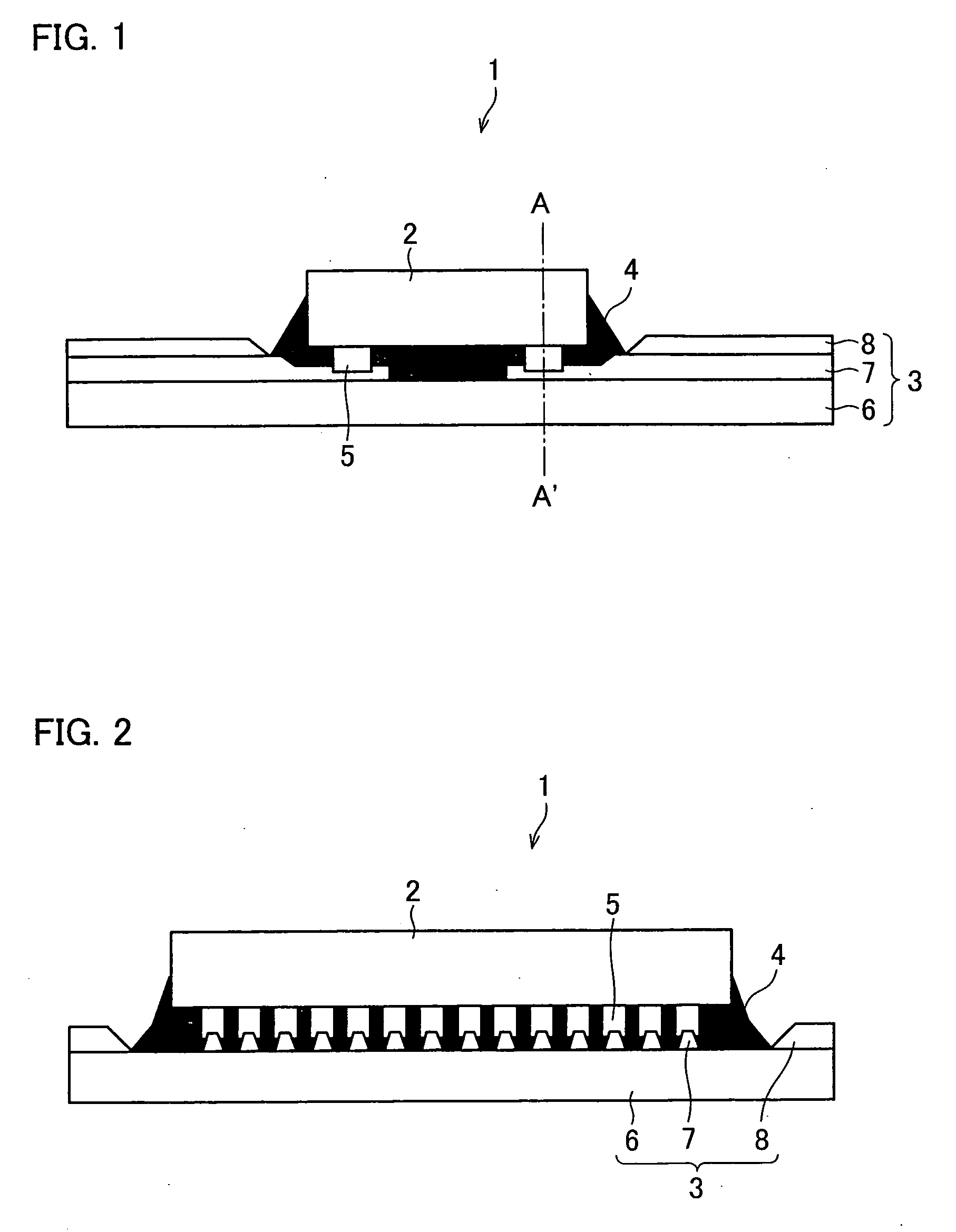
[0065] With reference to FIGS. 1 through 4(d), a first embodiment of the present invention is described below. FIG. 1 is a cross-sectional view schematically illustrating a structure of a semiconductor device of the present embodiment. Further, FIG. 2 is a cross-sectional view schematically illustrating the structure of the semiconductor device taken along line A-A′ of FIG. 1.

[0066] As illustrated in FIGS. 1 and 2, the semiconductor device 1 includes a semiconductor element (electronic component) 2 and a tape carrier (flexible wiring substrate) 3. The semiconductor element 2 is connected to the tape carrier 3. That is, the semiconductor element 2 is mounted on the tape carrier 3. Further, a gap between the tape carrier 3 and the semiconductor element 2 is sealed with an insulation resin 4. The present embodiment discusses, as an example, a COF-type semiconductor device having the above structure, in which the semiconductor element 2 is mounted on the tape carrier 3.

[0067] An examp...

second embodiment

[0093] With reference to FIGS. 1 through 3 and 5(d), a second embodiment of the present invention is described below. FIG. 1 is a cross-sectional view schematically illustrating a structure of a semiconductor device of the present embodiment. Further, FIG. 2 is a cross-sectional view schematically illustrating a structure of the semiconductor device taken along line A-A′ of FIG. 1.

[0094] As illustrated in FIG. 1, the semiconductor device 1 includes a semiconductor element 2 and a tape carrier 3. Compared to the first embodiment, the present embodiment describes a different fabricating method of the semiconductor device 1, though the structure of the semiconductor device 1 is the same. Thus, constituting elements having the same functions as those described in the first embodiment are indicated by the same reference numerals, and their explanations are omitted. In the present embodiment, the fabricating method of the semiconductor device 1 is mainly described. Further, the terms use...

third embodiment

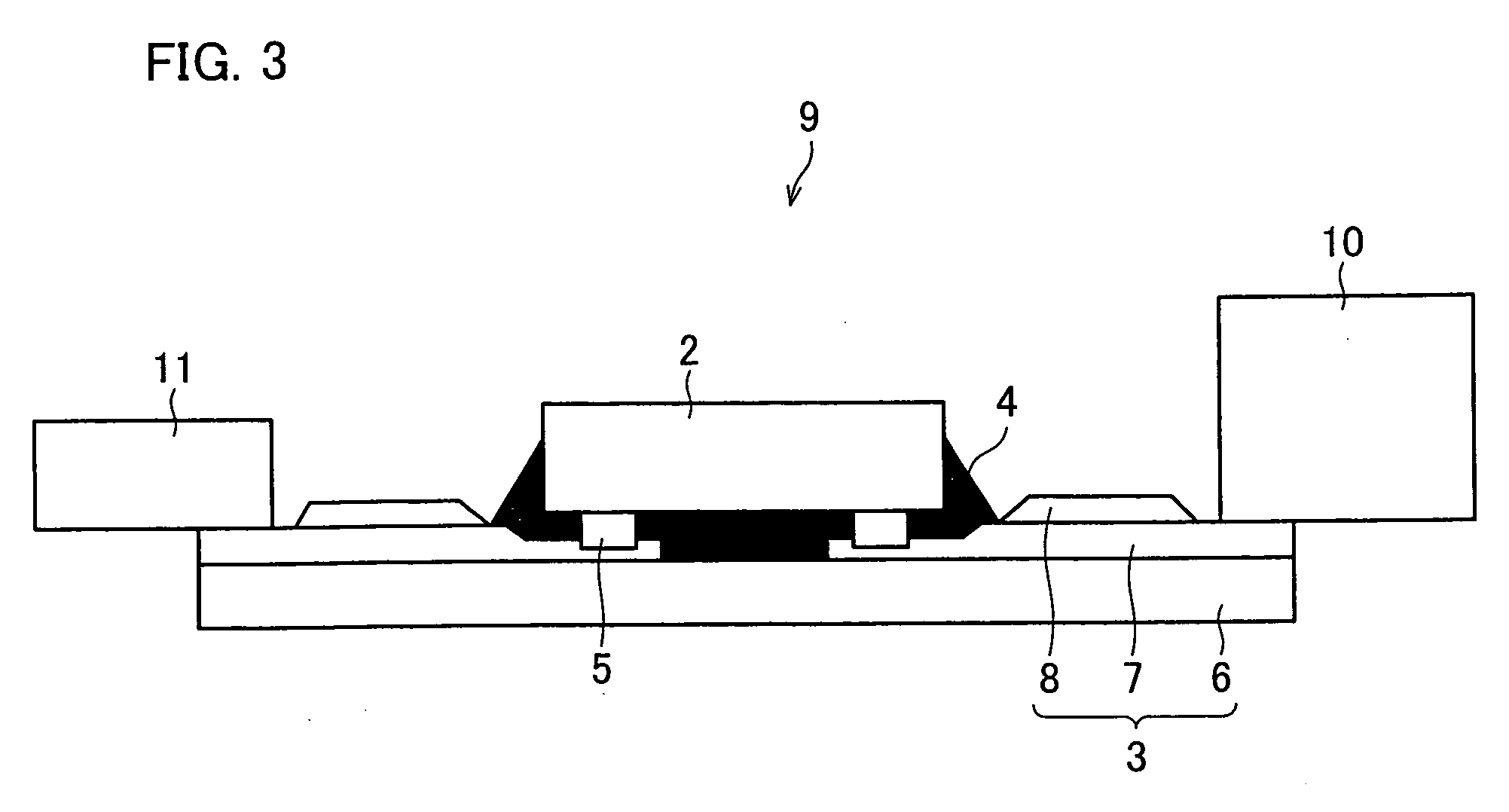
[0105] With reference to FIGS. 6 through 9(d), a third embodiment of the present invention is described below. FIG. 6 is a cross-sectional view schematically illustrating a structure of a semiconductor device of the present embodiment. Further, FIG. 7 is a cross-sectional view schematically illustrating a structure of the semiconductor device taken along line B-B′ of FIG. 6.

[0106] As illustrated in FIGS. 6 and 7, a semiconductor device 21 includes a semiconductor element 2 and a tape carrier (flexible wiring substrate) 23. The semiconductor element 2 is connected to and mounted on the tape carrier 23. Further, an insulation resin 4 is completely filled in a gap between the tape carrier 23 and the semiconductor element 2. The present embodiment discusses, as an example, a COF-type semiconductor apparatus having a structure in which the semiconductor element 2 is mounted on the tape carrier 23. Note that, constituting elements having the same functions as those described in the first...


PUM


Abstract

A flexible wiring substrate is provided which realizes a fine pitch of a wiring pattern and improves mechanical strength of the wiring pattern so as to prevent breaks or exfoliation of the wiring pattern. A flexible wiring substrate 3 of the present invention includes an insulation tape 6, and a wiring pattern 7 formed on the insulation tape 6. A thickness of the wiring pattern 7 is made thinner in a mounting region, where a semiconductor element is connected to, than in a non-mounting region.

Description

[0001] This Nonprovisional application claims priority under 35 U.S.C. § 119(a) on Patent Application No. 328173 / 2004 filed in Japan on Nov. 11, 2004, and on Patent Application No. 299402 / 2005 filed in Japan on Oct. 13, 2005, the entire contents of which are hereby incorporated by reference. FIELD OF THE INVENTION [0002] The present invention relates to a flexible wiring substrate, a semiconductor device and an electronic device which use the flexible wiring substrate, and a fabricating method of the flexible wiring substrate. The, present invention particularly relates to (i) a flexible wiring substrate on which a semiconductor element is mounted, (ii) a semiconductor device and an electronic device which use the semiconductor element, and (iii) a fabricating method of the flexible wiring substrate. BACKGROUND OF THE INVENTION [0003] A TCP (tape carrier package), a COF (chip on film), and the like are examples of a semiconductor device having a structure in which a semiconductor el...

Claims


Application Information

Patent Timeline
Patent Type & Authority Applications(United States)
IPC IPC(8): H01L23/495
CPCH01L21/563H01L23/4985H01L24/16H01L24/17H01L24/32H01L24/81H01L2224/13099H01L2224/13144H01L2224/16225H01L2224/27013H01L2224/32225H01L2224/73204H01L2224/81801H01L2224/83051H01L2224/83102H01L2224/92125H01L2924/01005H01L2924/01029H01L2924/01047H01L2924/0105H01L2924/01078H01L2924/01079H01L2924/01082H01L2924/01322H01L2924/14H01L2924/15153H01L2924/1517H05K1/111H05K1/189H05K3/244H05K2201/09736H05K2201/09745H05K2201/10674H05K2203/0369H01L2924/01006H01L2924/01033H01L2924/014H01L2924/0132H01L2224/16238H01L2224/81191H01L2224/81193H01L2224/2919H01L2924/1579H01L2224/29111H01L2224/13111H01L2924/00H01L2924/00012H01L2924/00014H01L2224/0554H01L2224/05568H01L2224/05573Y02P70/50H01L2224/05599H01L2224/0555H01L2224/0556H01L23/12
Inventor SEKO, TOSHIHARU
Owner SHENZHEN TOREY MICROELECTRONIC TECH CO LTD
Why Eureka
Try Eureka