

Plasma display panel
a technology of display panel and plasma, which is applied in the direction of gas discharge vessel/container, electrode, gas-filled discharge tube, etc., can solve the problems of undesired unavoidable increase in discharge voltage, and liable phosphor layer deterioration of facing discharge type pdp, etc., to achieve the effect of reducing discharge voltage and improving luminous efficiency
- Summary
- Abstract
- Description
- Claims
- Application Information
AI Technical Summary
Benefits of technology
Problems solved by technology
Method used
Image

Examples
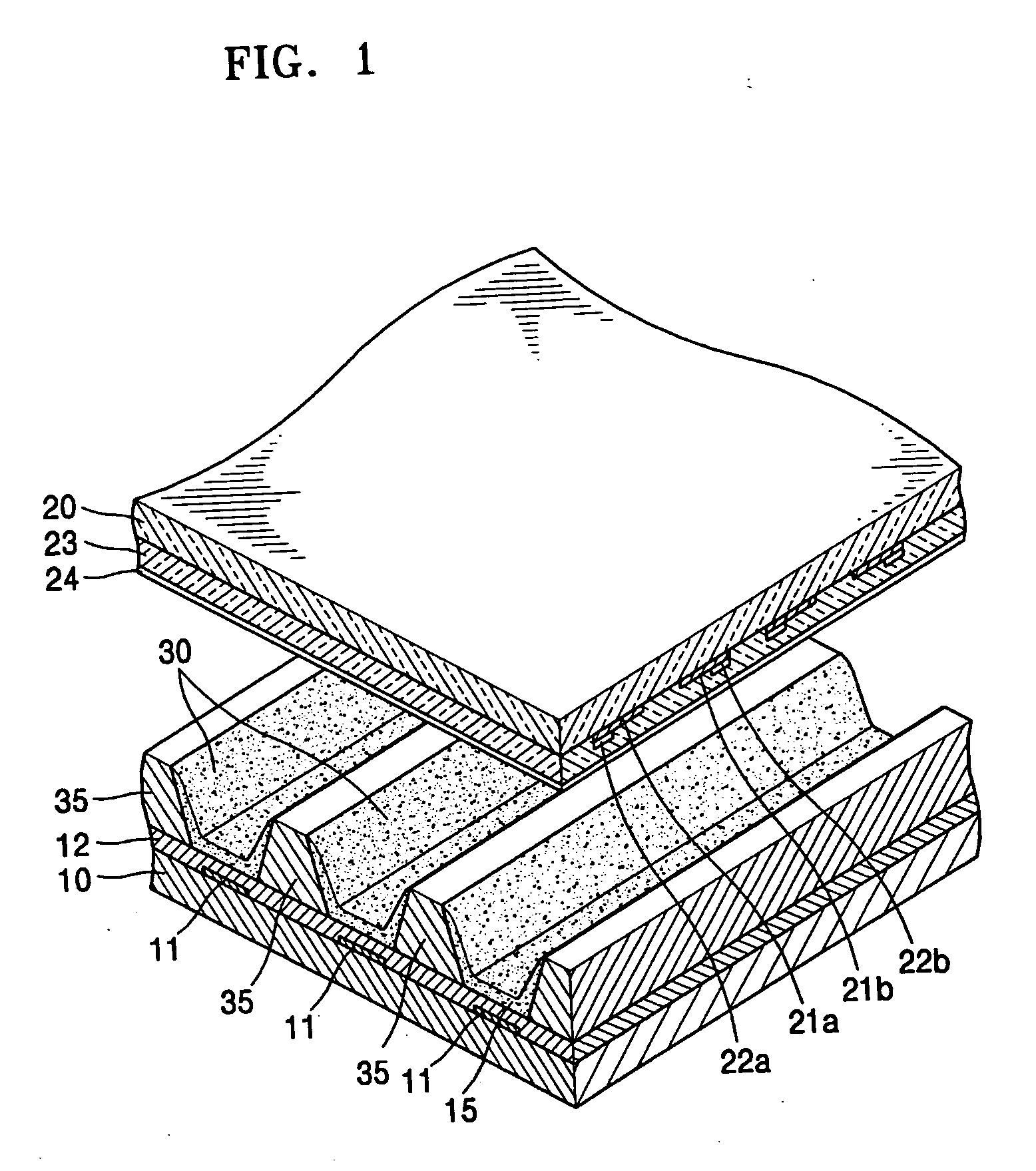
first embodiment
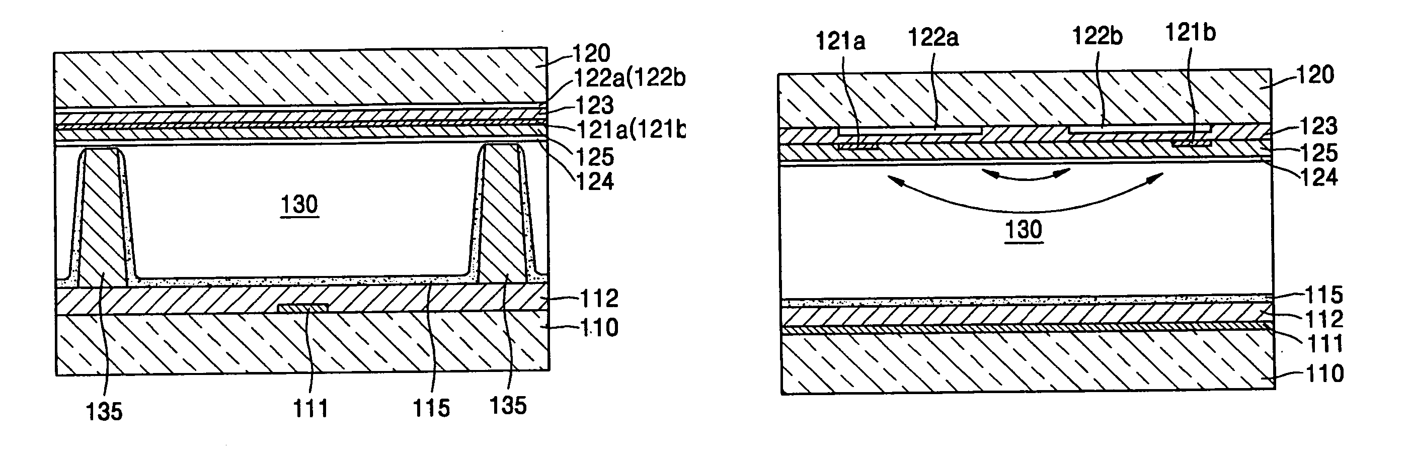
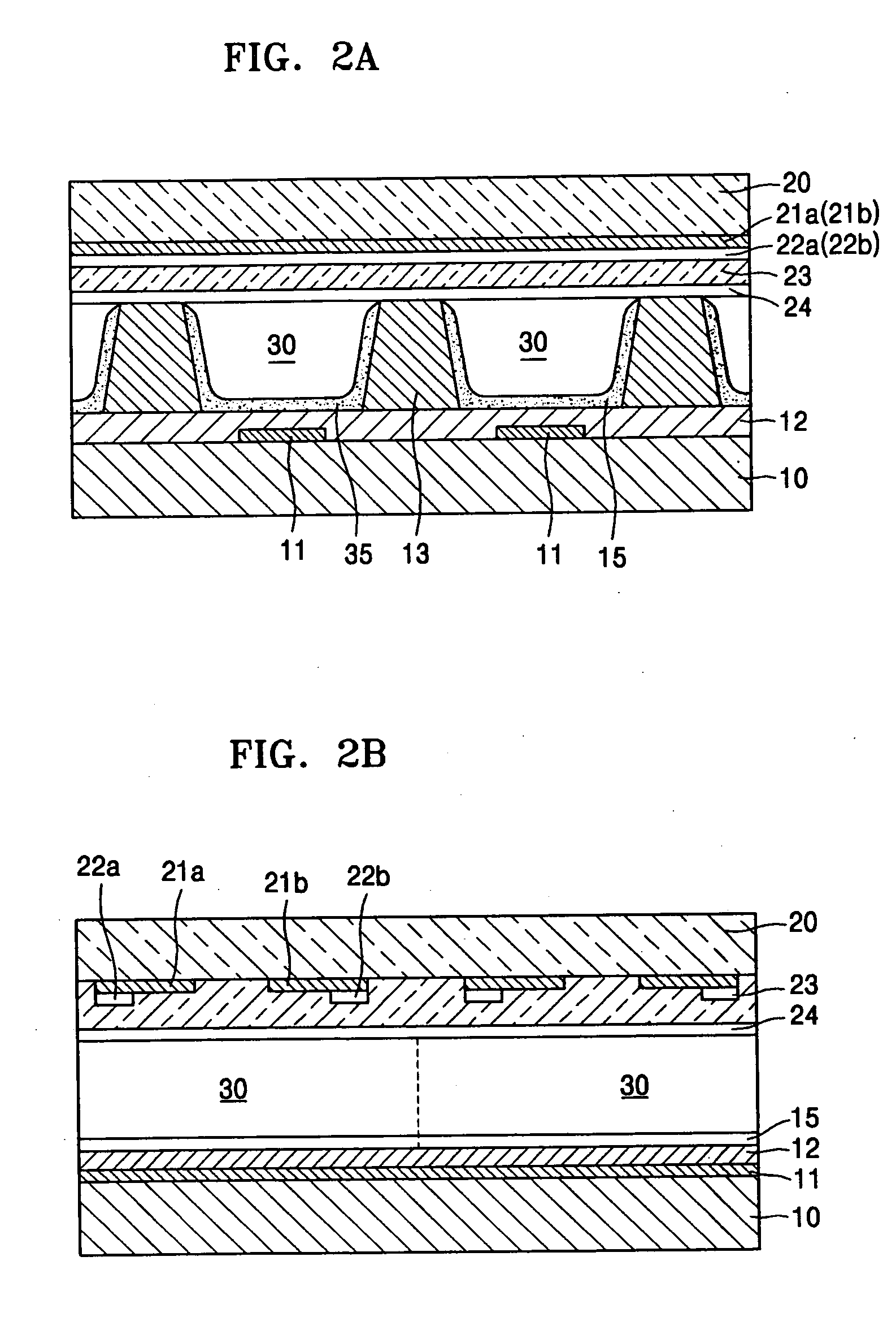
[0033]FIGS. 3A and 3B are cross-sectional views taken along horizontal and vertical directions of a PDP according to the present invention.
[0034] The PDP of FIGS. 3A and 3B is a reflective PDP, and is constructed in such a manner that a lower substrate 110 and an upper substrate 120 face each other with a discharge space formed therebetween. The lower substrate 110 and the upper substrate 120 are generally made of glass.
[0035] Multiple address electrodes 111 are formed on the lower substrate 110, and the address electrodes 111 are covered by a first dielectric layer 112. The discharge space is divided into multiple discharge cells 130 on the first dielectric layer 112, and multiple barriers 135 are spaced apart from each other by a predetermined gap, and are formed parallel to the address electrodes 111. The barriers 135 prevent electrical / optical interference between adjacent discharge cells 130. The discharge cells 130 are filled with a discharge gas emitting UV light by plasma d...
second embodiment
[0047]FIGS. 5A and 5B are cross-sectional views taken along horizontal and vertical directions of a PDP according to the present invention.
[0048] The PDP of FIGS. 5A and 5B is a transmissive PDP in which a lower substrate 210 and an upper substrate 220 face each other with a discharge space formed therebetween. Multiple address electrodes 221 are formed on the bottom surface of the upper substrate 220, and the address electrodes 221 are covered by a first dielectric layer 222.
[0049] The address electrodes 221 are preferably made of a transparent conductive material so as to cause the visible light emitted during discharge to be transmitted through the upper substrate 220. The address electrodes 221 may also be formed on the lower substrate 210.
[0050] The discharge space is divided into multiple discharge cells 230 so as to form multiple barriers 235 on the bottom surface of the first dielectric layer 222. A phosphor layer 225 is coated on the top surface of the first dielectric la...
third embodiment
[0054]FIGS. 6A and 6B are cross-sectional views taken along horizontal and vertical directions of a PDP according to the present invention.
[0055] The PDP of FIGS. 6A and 6B is a reflective PDP in which a lower substrate 310 and an upper substrate 320 are spaced apart by a predetermined interval and face each other with a discharge space formed therebetween. Multiple address electrodes 311 are formed on the lower substrate 320, and the address electrodes 311 are covered by a first dielectric layer 312. The discharge space is divided into the multiple discharge cells 330 so as to form multiple barriers 335 on the first dielectric layer 312. A phosphor layer 315 is coated on the top surface of the first dielectric layer 312 and lateral surfaces of the barriers 335, forming internal walls of the discharge cells 330 to a predetermined thickness. Although not shown in FIGS. 6A and 6B, a reflective layer for reflecting the visible light emitted from the discharge cells 330 toward the upper...
PUM
 Abstract
Description
Claims
Application Information