Memory block quality identification in a memory device

a memory device and quality identification technology, applied in the field of flash memory devices, can solve the problems of identifying the quality of memory blocks, the controller might have to handle a lot of overhead, and the integrated circuit manufacturer has to tag an entire memory block as bad

Active Publication Date: 2006-05-11
MICRON TECH INC
View PDF14 Cites 39 Cited by
  • Summary
  • Abstract
  • Description
  • Claims
  • Application Information

AI Technical Summary

Benefits of technology

[0009] The present invention encompasses a method for indicating the quality of defective memory blocks in a flash memory device. The method comprises performing a memory check to determine whether any locations in a block are defective. If a memory block is found to have a defect, a memory block quality indication is generated in response to the type of memory defect. This indication is stored in the memory device. In one embodiment, the quality indication is stored in a predetermined location of the defective memory block.
[0010] Using the quality indication, a system's error correction code scheme might be able to correct data errors resulting from the defect. If the ECC scheme is not capable of correcting the defect, the block can be considered unusable. If the system does not have an ECC scheme, the system can use the quality indication to decide what type of data to store in the defective block.

Problems solved by technology

Since there can be thousands of memory blocks in a typical memory device, this is considerable overhead for the controller to handle.
Another problem with marking memory locations as defective is that if certain locations in a flash memory device are marked as defective, the device might have to be discarded.
Additionally, integrated circuit manufacturers have to tag an entire memory block as bad even if it has only one bad bit in the field of 512 bytes.
Both of these problems reduce the manufacturer's part yield, thus increasing the cost of the memory devices in an industry operating on slim profit margins.
If the ECC scheme is not capable of correcting the defect, the block can be considered unusable.

Method used


Image

  • Memory block quality identification in a memory device
  • Memory block quality identification in a memory device
  • Memory block quality identification in a memory device

Examples


Embodiment Construction

[0016] In the following detailed description of the invention, reference is made to the accompanying drawings that form a part hereof and in which is shown, by way of illustration, specific embodiments in which the invention may be practiced. In the drawings, like numerals describe substantially similar components throughout the several views. These embodiments are described in sufficient detail to enable those skilled in the art to practice the invention. Other embodiments may be utilized and structural, logical, and electrical changes may be made without departing from the scope of the present invention. The following detailed description is, therefore, not to be taken in a limiting sense, and the scope of the present invention is defined only by the appended claims and equivalents thereof.

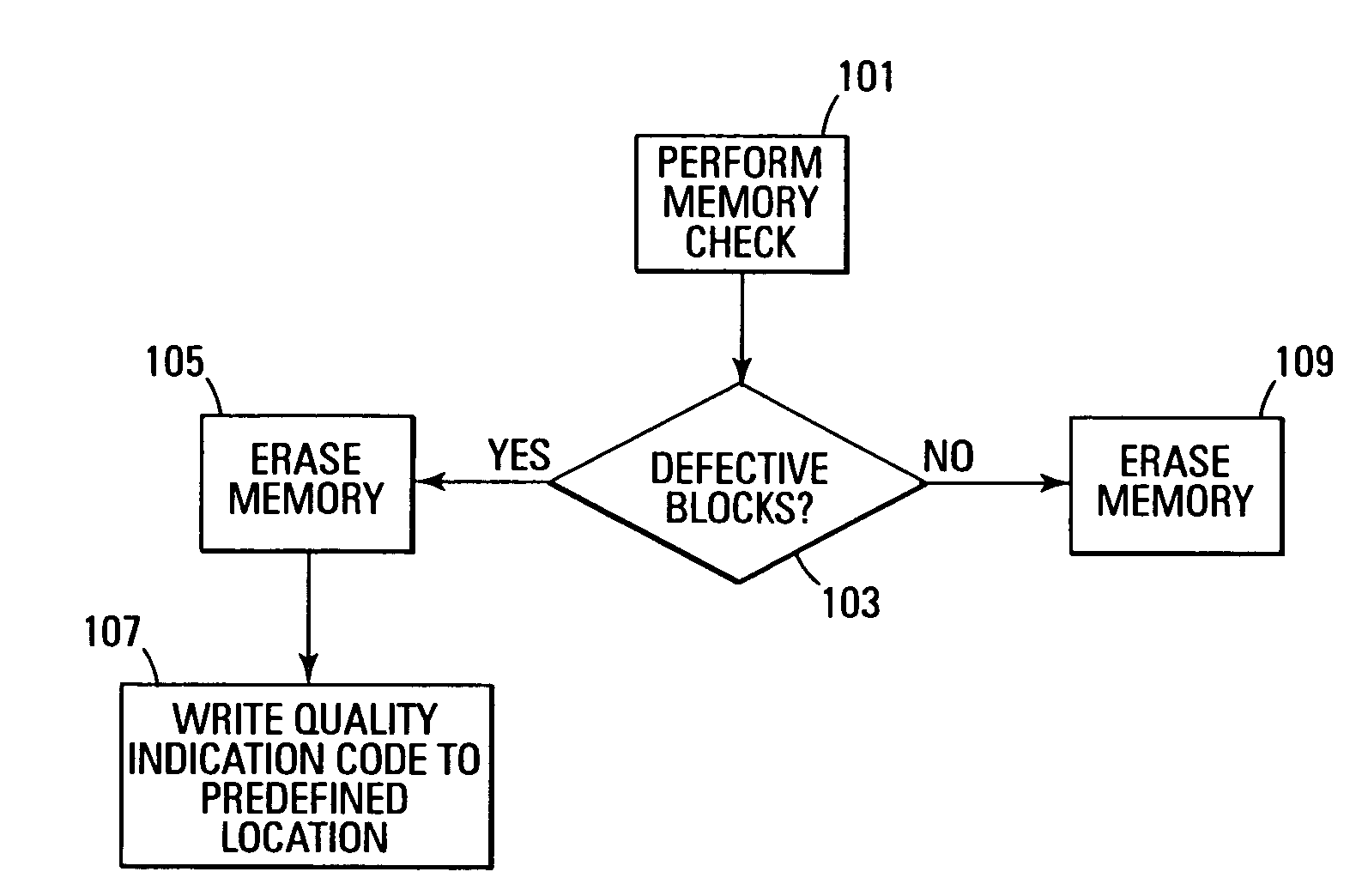
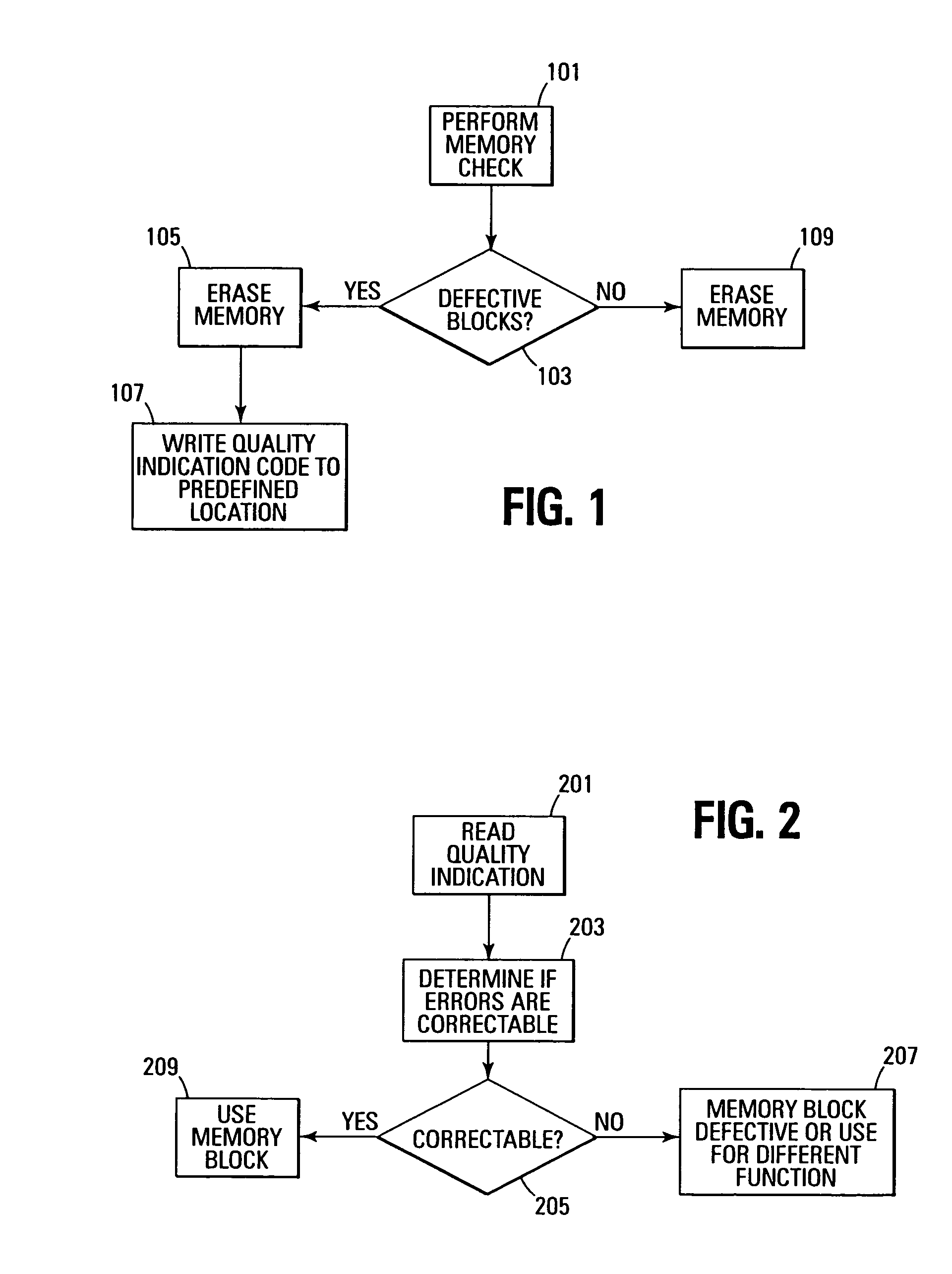
[0017]FIG. 1 illustrates a flowchart of one embodiment of a method for generating a memory block quality indication in a flash memory device. In one embodiment, this method would be performed d...


PUM


Abstract

If a memory block in a flash memory device is found to have a defect, a memory block quality indication is generated in response to the type of memory defect. This indication is stored in the memory device. In one embodiment, the quality indication is stored in a predetermined location of the defective memory block. Using the quality indication, it can be determined if a system's error correction code scheme is capable of correcting data errors resulting from the defect.

Description

TECHNICAL FIELD OF THE INVENTION [0001] The present invention relates generally to memory devices and in particular the present invention relates to a flash memory devices. BACKGROUND OF THE INVENTION [0002] Memory devices are typically provided as internal, semiconductor, integrated circuits in computers or other electronic devices. There are many different types of memory including random-access memory (RAM), read only memory (ROM), dynamic random access memory (DRAM), synchronous dynamic random access memory (SDRAM), and flash memory. [0003] Flash memory devices have developed into a popular source of non-volatile memory for a wide range of electronic applications. Flash memory devices typically use a one-transistor memory cell that allows for high memory densities, high reliability, and low power consumption. Common uses for flash memory include personal computers, personal digital assistants (PDAs), digital cameras, and cellular telephones. Program code and system data such as ...

Claims


Application Information

Patent Timeline
Patent Type & Authority Applications(United States)
IPC IPC(8): G11C16/06G11C29/00G11C7/00
CPCG06F11/073G06F11/0775G11C16/04G11C2029/4402G11C29/44G11C2029/1208G11C29/26G06F3/0604G06F3/0631G06F3/064G06F3/0679G06F11/1068G11C29/52
Inventor ROOHPARVAR, FRANKIE F.
Owner MICRON TECH INC
Why Eureka
Try Eureka