Interconnect structure to reduce stress induced voiding effect

a technology of interconnection structure and stress-induced voiding, which is applied in the direction of semiconductor devices, semiconductor/solid-state device details, electrical devices, etc., can solve the problems of increasing reducing the size of cmos devices, and reducing the number of vias, so as to reduce the formation of metal voids.

Inactive Publication Date: 2006-05-11
TAIWAN SEMICON MFG CO LTD
View PDF5 Cites 0 Cited by
  • Summary
  • Abstract
  • Description
  • Claims
  • Application Information

AI Technical Summary

Benefits of technology

[0005] These and other problems are generally solved or circumvented, and technical advantages are generally achieved, by preferred embodiments of the present invention, which provides a method and an apparatus for reducing metal void formation caused by stress migration or method relaxation.

Problems solved by technology

Significant challenges, however, are faced as the sizes of CMOS devices continue to decrease.
One such challenge is the fabrication of interconnect structures, e.g., vias.
The vias, particularly vias connecting a metal lead with a thin metal line to an underlying conductive layer, are frequently subjected to significant stress.
The stressed-induced voids may significantly affect the electrical characteristics of the via and may cause the semiconductor structure to fail.

Method used


Image

  • Interconnect structure to reduce stress induced voiding effect
  • Interconnect structure to reduce stress induced voiding effect
  • Interconnect structure to reduce stress induced voiding effect

Examples


Embodiment Construction

[0016] The making and using of the presently preferred embodiments are discussed in detail below. It should be appreciated, however, that the present invention provides many applicable inventive concepts that can be embodied in a wide variety of specific contexts. The specific embodiments discussed herein are merely illustrative of specific ways to make and use the invention, and do not limit the scope of the invention.

[0017] Embodiments of the present invention provide methods and device designs for eliminating or reducing stress-induced voids. Embodiments of the present invention are described in reference to forming a via to electrically couple an upper-layer metal contact to an underlying conductive region. Specific shapes and configurations are disclosed, however, it should be appreciated by one of ordinary skill in the art that other shapes and configurations may be used.

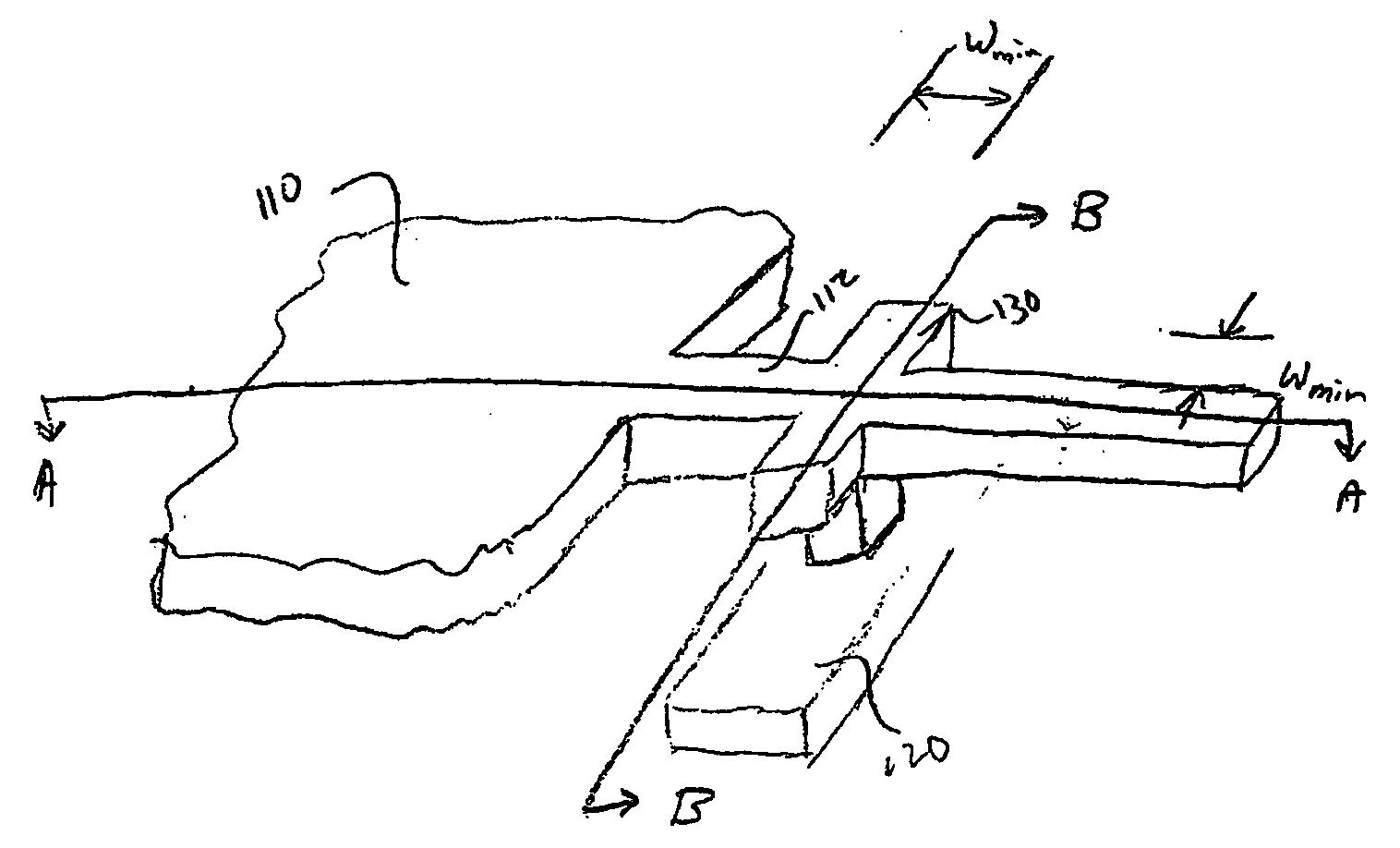
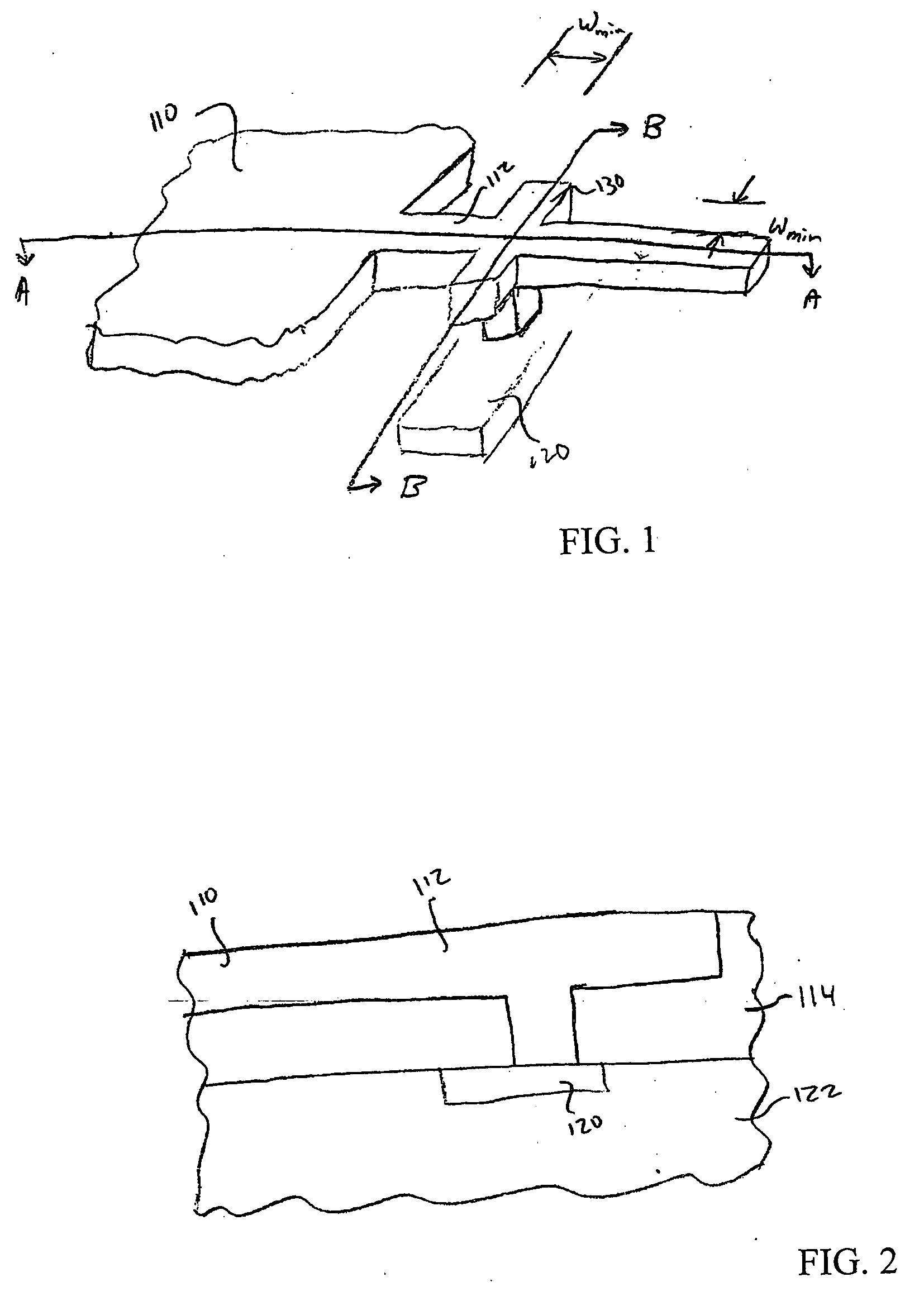
[0018] Referring now to FIGS. 1-3, FIG. 1 shows a perspective view of an interconnect structure, and FIGS...


PUM


Abstract

An interconnect structure that may reduce or eliminate stress induced voids is provided. In an embodiment, a via is formed below a conductive line to provide an electrical connection to an underlying conductive region. The conductive line includes a widened region above the via. The widened region serves to reduce or eliminate stress induced voids between the via and the underlying conductive region. In another embodiment, one or more redundant lines are formed extending from a conductive region, such as a contact pad, such that the redundant line does not electrically couple the conductive region to an underlying conductive region. In a preferred embodiment, the redundant lines extend from a conductive region on a side adjacent to a side having a conductive line coupled to a via.

Description

TECHNICAL FIELD[0001] The present invention generally relates to a method of metallization in the fabrication of integrated circuits, and more particularly, to a method and an apparatus for reducing metal void formation caused by stress migration or metal relaxation in the manufacture of integrated circuits. BACKGROUND [0002] Complementary metal-oxide-semiconductor (CMOS) technology is the dominant semiconductor technology used for the manufacture of ultra-large scale integrated (ULSI) circuits today. Size reduction of the semiconductor structures has provided significant improvement in the speed, performance, circuit density, and cost per unit function of semiconductor chips over the past few decades. Significant challenges, however, are faced as the sizes of CMOS devices continue to decrease. [0003] One such challenge is the fabrication of interconnect structures, e.g., vias. CMOS devices typically include semiconductor structures, such as transistors, capacitors, resistors, and t...

Claims


Application Information

Patent Timeline
Patent Type & Authority Applications(United States)
IPC IPC(8): H01L21/4763
CPCH01L21/76816H01L21/76838H01L23/5226H01L23/528H01L21/76879H01L2924/0002H01L2924/00
Inventor WANG, CHIEN-JUNG
Owner TAIWAN SEMICON MFG CO LTD
Why Eureka
Try Eureka