
Voltage down converter

a voltage converter and converter circuit technology, applied in the direction of electric variable regulation, static storage, instruments, etc., can solve the problems of low response speed, unstable output voltage, and the inability of the voltage converter circuit to track the relatively fast changes in the requested current, and achieve the effect of low response tim

Inactive Publication Date: 2006-05-18
STMICROELECTRONICS SRL
View PDF5 Cites 19 Cited by
  • Summary
  • Abstract
  • Description
  • Claims
  • Application Information

AI Technical Summary

Benefits of technology

[0014] Another object of the present invention is to provide a voltage down converter that is stable, with relatively low response times, and which permits the regulation of the down-converted voltage when the loads dynamically change.

Problems solved by technology

A problem of such a conventional device is the output voltage stability (response speed is limited by heavy frequency compensation), because capacitive loads coupled to the internal voltage supply line dynamically vary depending on the operations performed on the memory device (different circuits may be activated, depending on the operations).
The voltage down converter circuit cannot track the relatively fast changes in the requested current.
However, this further, open-loop solution, in which the internal voltage supply line is decoupled from the voltage regulator, does not permit there to be maintained the desired down-converted voltage at the internal voltage supply line because of the dynamical variations of the loads during the operation of the memory device (the regulation characteristic of the circuit has in fact a relatively high slope).
In addition, in both the above-described conventional devices, transients in the down-converted voltage value caused by variations of the loads can have a relatively long duration, at best some tens of nanoseconds.

Method used


Image

  • Voltage down converter
  • Voltage down converter
  • Voltage down converter

Examples


Embodiment Construction

[0024] Preferred embodiments of the present invention will be described in detail hereinbelow with reference to the attached drawings.

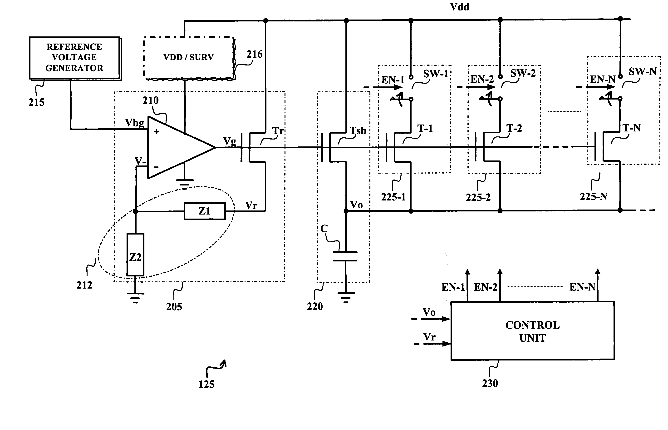
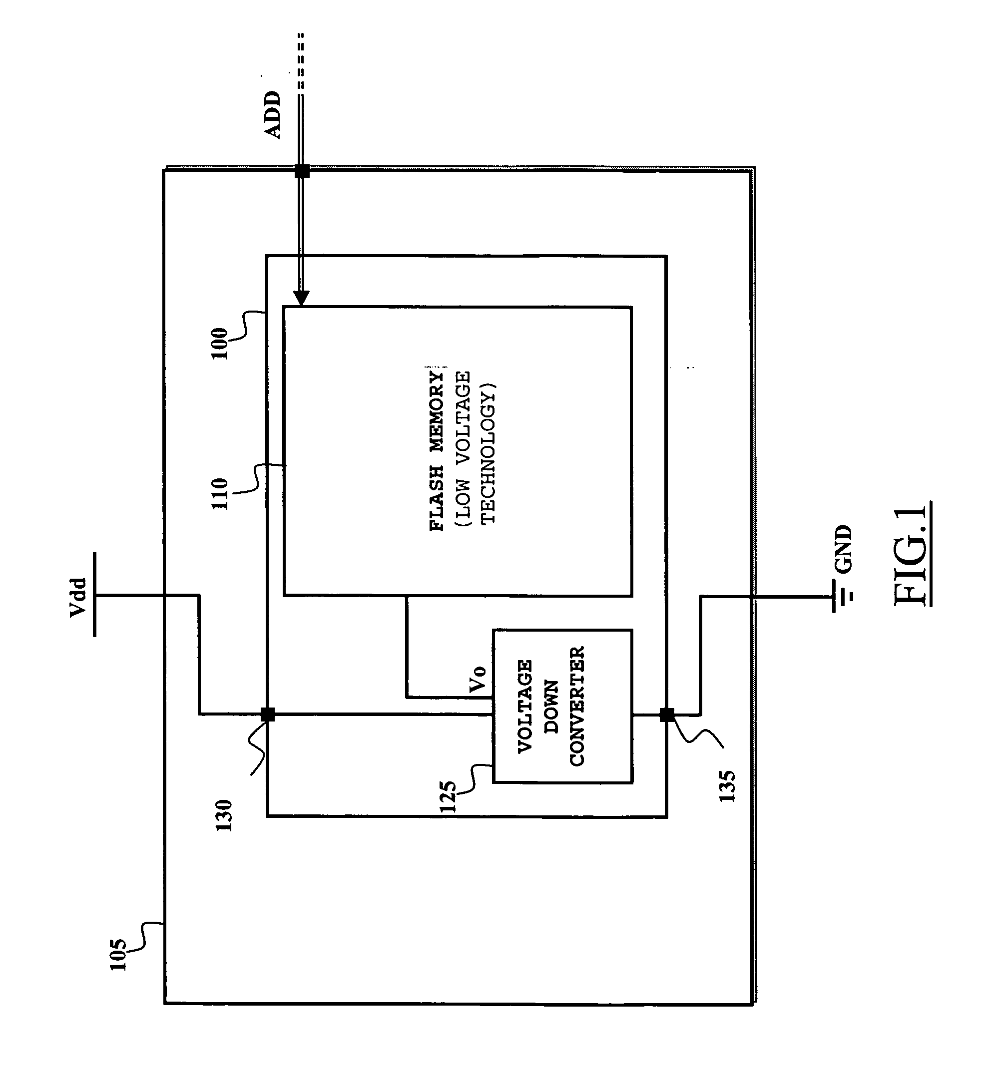
[0025]FIG. 1 illustrates an integrated circuit 100 comprising a semiconductor memory device, particularly a non-volatile semiconductor memory 110, realized in a low-voltage manufacturing technology (for example, an E2PROM of flash type). The integrated circuit 100 is integrated in a chip 105 of semiconductor material. The flash memory 110 typically includes a matrix of memory cells (for example consisting of floating gate MOS transistors), and a variety of circuit blocks such as decoders used to select the memory cells (for example in response to a corresponding address ADD received from the outside), and read / write circuits that are used to read / update the contents of the selected memory cells. Particularly, the read / write circuits include the components necessary to execute read and write (and, possibly, erase) operations on the selected memory cel...


PUM


Abstract

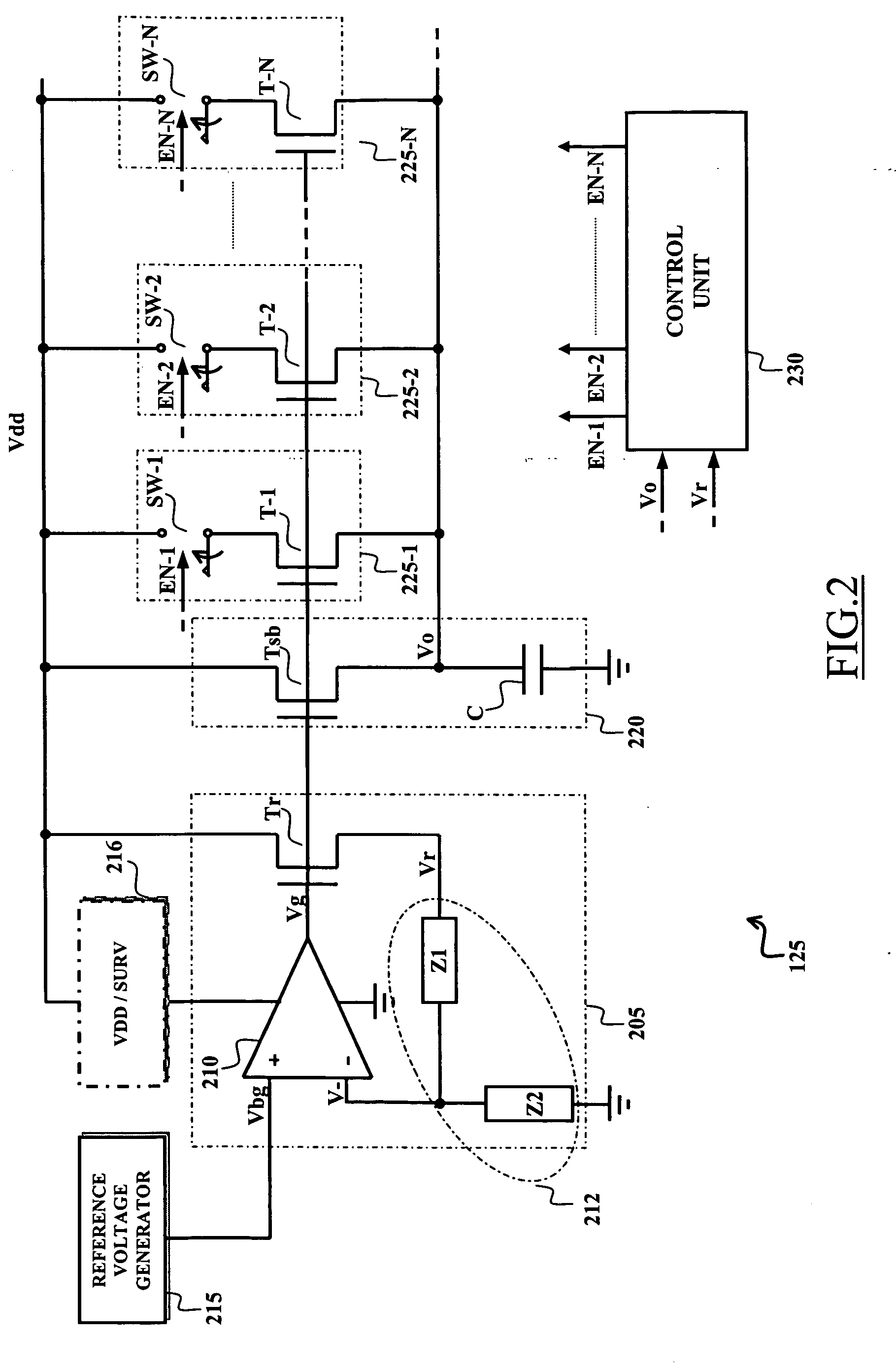
A voltage down converter is provided that includes a voltage regulator and voltage driver circuit branches. The voltage regulator receives a first voltage, has a regulation node providing a regulated second voltage that is lower than the first voltage, and has a control node providing a control voltage corresponding to the second voltage. One voltage driver circuit branch receives the first voltage and includes a variable-conductivity element having a control terminal coupled to the control node for controlling a current sunk by the variable-conductivity element. This one voltage driver circuit branch has a voltage supply node supplying a down-converted voltage corresponding to the second voltage. At least one additional voltage driver circuit branch receives the first voltage and is coupled to the voltage supply node. The additional voltage driver circuit branch includes a further variable-conductivity element having a control terminal coupled to the control node for controlling a current sunk by the further variable-conductivity element, and a switching circuit for selectively enabling the further variable-conductivity element so as to keep the down-converted voltage at a prescribed value depending on the regulated second voltage.

Description

CROSS-REFERENCE TO RELATED APPLICATIONS [0001] This application is based upon and claims priority from prior European Patent Application No. 4 105 351.3, filed Oct. 28, 2004, the entire disclosure of which is herein incorporated by reference. FIELD OF THE INVENTION [0002] The present invention relates to a voltage down converter, and in particular to a voltage down converter for use in a semiconductor memory device, such as a non-volatile memory device. BACKGROUND OF THE INVENTION [0003] Nowadays, many semiconductor memory devices are designed so as to be adapted to operate with low supply voltages, such as supply voltages down to 1.8 V. Considering, for example, a non-volatile semiconductor memory device (e.g., an E2PROM of flash type), the use of a relatively low supply voltage permits the use of technologies with very thin gate oxide layers (e.g., with a thickness lower than 50 Å). Accordingly, it is possible to implement semiconductor memory devices that are more compact, and th...

Claims


Application Information

Patent Timeline
IPC IPC(8): G05F1/10
CPCG05F3/262G11C5/147
Inventor PISASALE, MICHELANGELOGAIBOTTI, MAURIZIOLA PLACA, MICHELE
Owner STMICROELECTRONICS SRL
Learn More