Method for engineering hybrid orientation/material semiconductor substrate

a technology of hybrid orientation and semiconductor substrate, applied in the direction of semiconductor/solid-state device manufacturing, basic electric elements, electric devices, etc., can solve the problems that the current technology of forming cmos devices on the same substrate/platform will face severe limitations in the future, and achieve the effect of reducing repetition

Inactive Publication Date: 2006-05-18
CHARTERED SEMICONDUCTOR MANUFACTURING
View PDF22 Cites 97 Cited by
  • Summary
  • Abstract
  • Description
  • Claims
  • Application Information

AI Technical Summary

Benefits of technology

[0023] The above and below advantages and features are of representative embodiments only, and are not exhaustive and / or exclusive. They are presented only to assist in understanding the invention. It should be understood that they are not representative of all the inventions defined by the claims, to be considered limitations on the invention as defined by the claims, or limitations on equivalents to the claims. For instance, some of these advantages may be mutually contradictory, in that they cannot be simultaneously present in a single embodiment. Similarly, some advantages are applicable to one aspect of the invention, and inapplicable to others. Furthermore, certain aspects of the claimed invention have not been discussed herein. However, no inference should be drawn regarding those discussed herein relative to those not discussed herein other than for purposes of space and reducing repetition. Thus, this summary of features and advantages should not be considered dispositive in determining equivalence. Additional features and advantages of the invention will become apparent in the following description, from the drawings, and from the claims.

Problems solved by technology

In addition, due to the different substrate requirements for carrier mobility enhancement in NMOS and PMOS devices, the current technology for forming CMOS devices on the same substrate / platform will face severe limitations in the future.

Method used


Image

  • Method for engineering hybrid orientation/material semiconductor substrate
  • Method for engineering hybrid orientation/material semiconductor substrate
  • Method for engineering hybrid orientation/material semiconductor substrate

Examples


Embodiment Construction

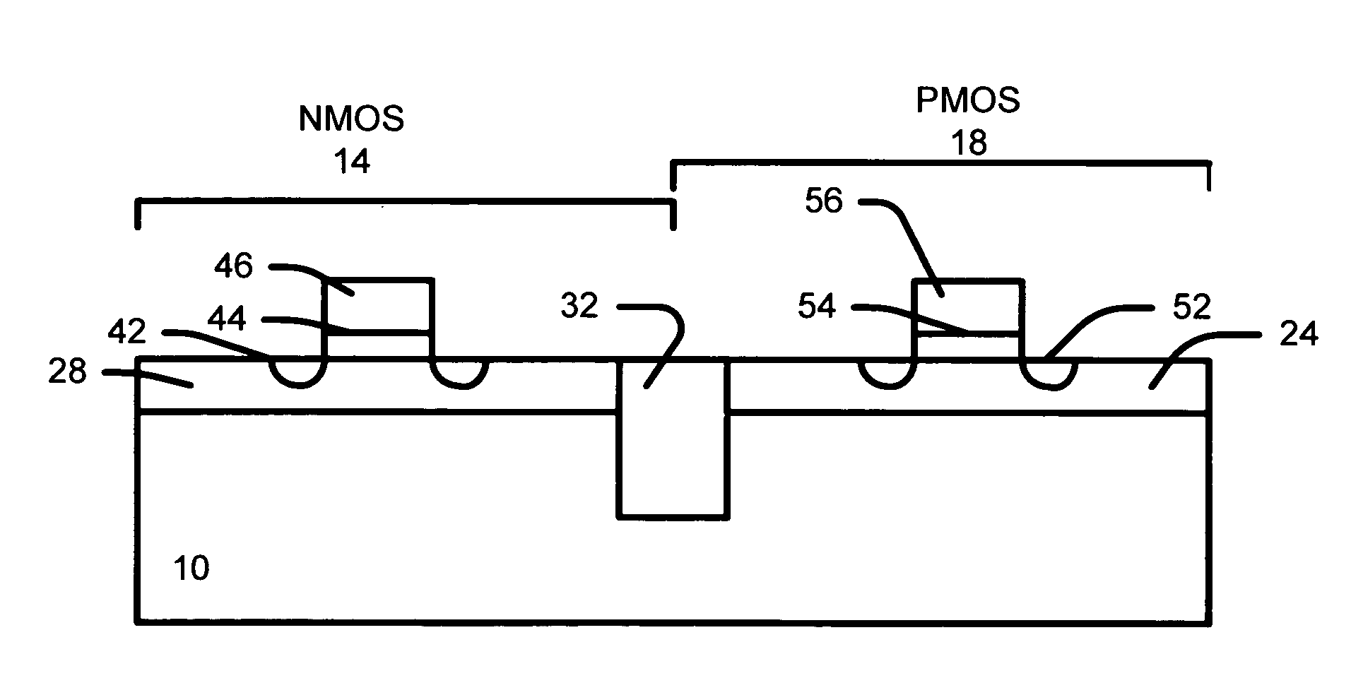
[0026] The present invention will be described in detail with reference to the accompanying drawings. The present invention provides a method of forming a semiconductor structure with different materials in the PMOS and NMOS active areas.

[0027] A. Substrate

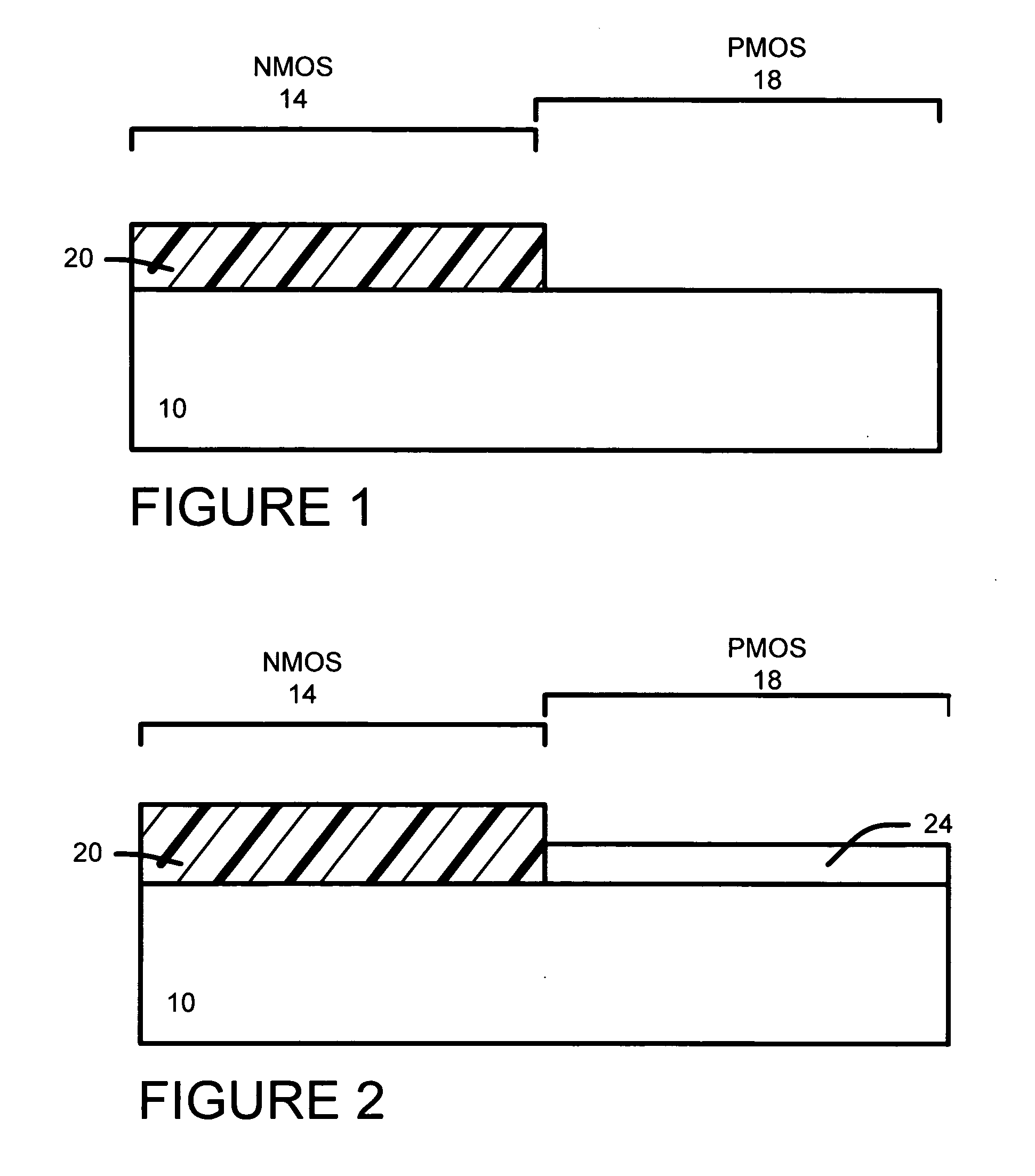
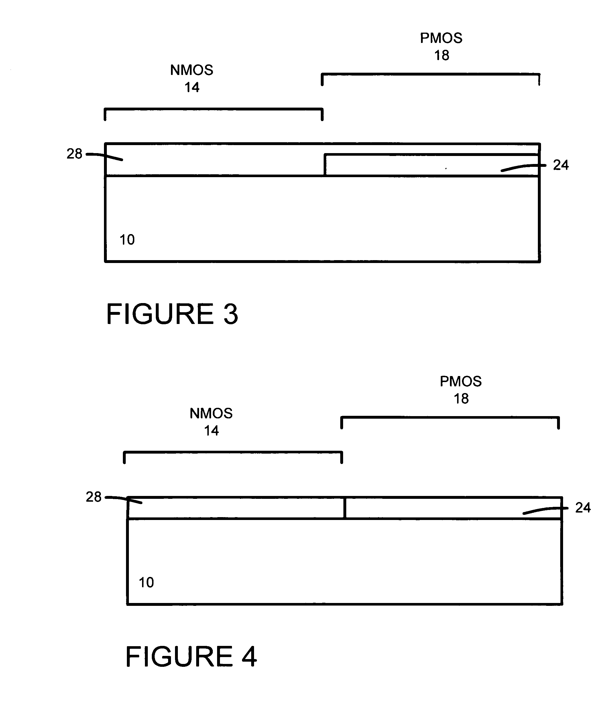
[0028] Referring to FIG. 1, we provide a substrate 10. The substrate has a NMOS area 14 and a PMOS area 18.

[0029] The substrate 10 can be comprised of a silicon wafer, a silicon on insulator substrate (SOI), strained silicon or SiGe.

[0030] The substrate 10 can be comprised of silicon with a (010) or (110) or (100) orientation. It is preferable that the substrate 10 comprises silicon with a (100) orientation. The substrate preferably has thickness between 500 and 1000 micrometers (um). The substrate is preferably doped with P or B at a concentration between 1×10¹⁵ and 1×10¹⁶ / cm3.

[0031] The substrate can also be comprised of a SOI substrate. The SOI substrate comprised of a low layer, an insulating layer, and an upper silicon l...


PUM


Abstract

The embodiments provide a structure and a method of manufacturing a semiconductor structure that has a different material in the area where PMOS devices will be formed than in the area where NMOS devices will be formed which is characterized as follows. An embodiment comprises the following steps. A substrate is provided. The substrate has a NMOS area and a PMOS area. We form a NMOS mask over the NMOS area. We form a first semiconductor layer over the PMOS area. We remove the mask. We form a second semiconductor layer over the NMOS area. Then we form an isolation region in the substrate between at least portions of the NMOS and the PMOS areas. We form PMOS devices in the PMOS area and form NMOS devices in the NMOS area.

Description

BACKGROUND OF INVENTION [0001] 1) Field of the Invention [0002] This invention relates generally to the structure and fabrication of semiconductor structures and more particularly to the fabrication of a semiconductor structure with different materials in the PMOS and NMOS active areas. [0003] 2) Description of the Prior Art [0004] Mobility degradation is a major concern for transistor scaling due to higher channel doping, higher vertical field, and the use of high-k gate dielectric materials. In addition, due to the different substrate requirements for carrier mobility enhancement in NMOS and PMOS devices, the current technology for forming CMOS devices on the same substrate / platform will face severe limitations in the future. For e.g., it is known that hole mobility can be enhanced with the use of a silicon-germanium (SiGe) channel. [0005] The relevant technical developments in the patent literature can be gleaned by considering the following. [0006] U.S. Pat. No. 6,774,409 Baba, ...

Claims


Application Information

Patent Timeline
Patent Type & Authority Applications(United States)
IPC IPC(8): H01L21/8228
CPCH01L21/823807
Inventor CHONG, YUNG FUHSIA, LIANG CHOOANG, CHEW HOE
Owner CHARTERED SEMICONDUCTOR MANUFACTURING
Why Eureka
Try Eureka