Semiconductor device having improved power density

a technology of semiconductor devices and power density, which is applied in the direction of semiconductor devices, semiconductor/solid-state device details, electrical apparatus, etc., can solve the problems of not significantly increasing the cost of manufacturing integrated circuits, and achieve the effects of increasing power density in mos devices, increasing on-resistance, and decreasing device breakdown voltag

Active Publication Date: 2006-06-01
BELL SEMICON LLC
View PDF34 Cites 55 Cited by
  • Summary
  • Abstract
  • Description
  • Claims
  • Application Information

AI Technical Summary

Benefits of technology

[0007] The present invention meets the above-noted need by providing techniques for beneficially increasing power density in an MOS device, without increasing on-resistance or decreasing breakdown voltage in the device. For example, in accordance with an illustrative embodiment of the present invention, an LDMOS is formed having a buried layer which is arranged so as to minimize HCI while controlling at least an on-resistance, maximum drain current, and / or breakdown voltage in the device so as to achieve a desired electrical performance in the device. Moreover, the techniques of the present invention can be used to fabricate an integrated circuit including, for example, one or more LDMOS devices, using conventional MOS compatible process technology. Consequently, the cost of manufacturing the integrated circuit is not significantly increased.

Problems solved by technology

Consequently, the cost of manufacturing the integrated circuit is not significantly increased.

Method used


Image

  • Semiconductor device having improved power density
  • Semiconductor device having improved power density
  • Semiconductor device having improved power density

Examples


Embodiment Construction

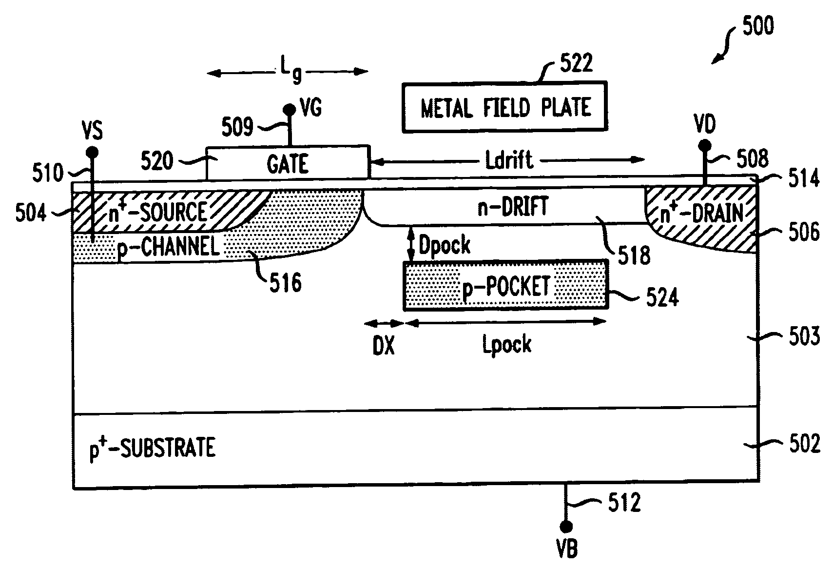
[0021] The present invention will be described herein in the context of an illustrative complementary MOS (CMOS) IC fabrication technology suitable for forming discrete LDMOS transistors, as well as circuits and / or other devices. It should be appreciated, however, that the present invention is not limited to the fabrication of this or any particular circuit or other device. Rather, the invention is more generally applicable to an improved MOS device which is advantageously configured to optimize a power density in the device, without significantly impacting breakdown voltage and / or HCI degradation. Moreover, the improved device is fully compatible with an MOS process technology.

[0022] Although implementations of the present invention are described herein with specific reference to an LDMOS device, it is to be appreciated that the techniques of the present invention are similarly applicable to other devices, as will be understood by those skilled in the art. Furthermore, although th...


PUM


Abstract

An MOS device is formed including a semiconductor layer of a first conductivity type, and source and drain regions of a second conductivity type formed in the semiconductor layer proximate an upper surface of the semiconductor layer. The source and drain regions are spaced apart relative to one another. A drift region of the second conductivity type is formed in the semiconductor layer proximate the upper surface of the semiconductor layer and at least partially between the source and drain regions, the drift region having an impurity doping concentration greater than about 2.0e12 atoms / cm2. An insulating layer is formed on at least a portion of the upper surface of the semiconductor layer. The device further includes a gate formed on the insulating layer at least partially between the source and drain regions, and a buried layer of the first conductivity type formed in the semiconductor layer in close relative proximity to and beneath at least a portion of the drift region. A substantially vertical distance between the buried layer and the drift region, and / or one or more physical dimensions of the buried layer are configured so as to optimize a power density of the device relative to at least one of an on-resistance and a maximum drain current of the device.

Description

FIELD OF THE INVENTION [0001] The present invention relates generally to semiconductor devices, and more particularly relates to techniques for achieving increased power density in a semiconductor device without significantly increasing hot carrier injection (HCI) and / or decreasing breakdown voltage in the device. BACKGROUND OF THE INVENTION [0002] Power semiconductor devices, including lateral diffused metal-oxide semiconductor (LDMOS) devices, are employed in a wide variety of applications, such as, for example, power amplification and switching. Although these power devices can achieve high efficiency, linearity and power gain with sufficient reliability when biased at relatively high drain bias voltages (e.g., up to about 30 volts), it is desirable to increase a power density (PDEN) in theses devices. Increased power density generally results in smaller device areas, which translates into lower cost per watt. Furthermore, increasing the power density without also increasing para...

Claims


Application Information

Patent Timeline
Patent Type & Authority Applications(United States)
IPC IPC(8): H01L23/58
CPCH01L29/1083H01L29/402H01L29/7835
Inventor BUDE, JEFF D.KIZILYALLI, ISIK C.SMITH, KENT
Owner BELL SEMICON LLC
Why Eureka
Try Eureka