Semiconductor memory device having a decoupling capacitor

a memory device and capacitor technology, applied in semiconductor devices, capacitors, electrical equipment, etc., can solve the problems of difficult manufacturing of cell capacitors, difficult to realize high capacitance using plate-type dielectric films such as gate-oxide films, and generally occurring decoupling noise, etc., to achieve the effect of reducing the nois

Inactive Publication Date: 2006-06-01
SAMSUNG ELECTRONICS CO LTD
View PDF2 Cites 13 Cited by
  • Summary
  • Abstract
  • Description
  • Claims
  • Application Information

AI Technical Summary

Benefits of technology

[0013] In general, exemplary embodiments of the invention include highly-...

Problems solved by technology

The coupling noise generally occurs due to the parasitic capacitance of a parasitic capacitor.
Thus, it has been difficult to realize a high c...

Method used


Image

  • Semiconductor memory device having a decoupling capacitor
  • Semiconductor memory device having a decoupling capacitor
  • Semiconductor memory device having a decoupling capacitor

Examples


Embodiment Construction

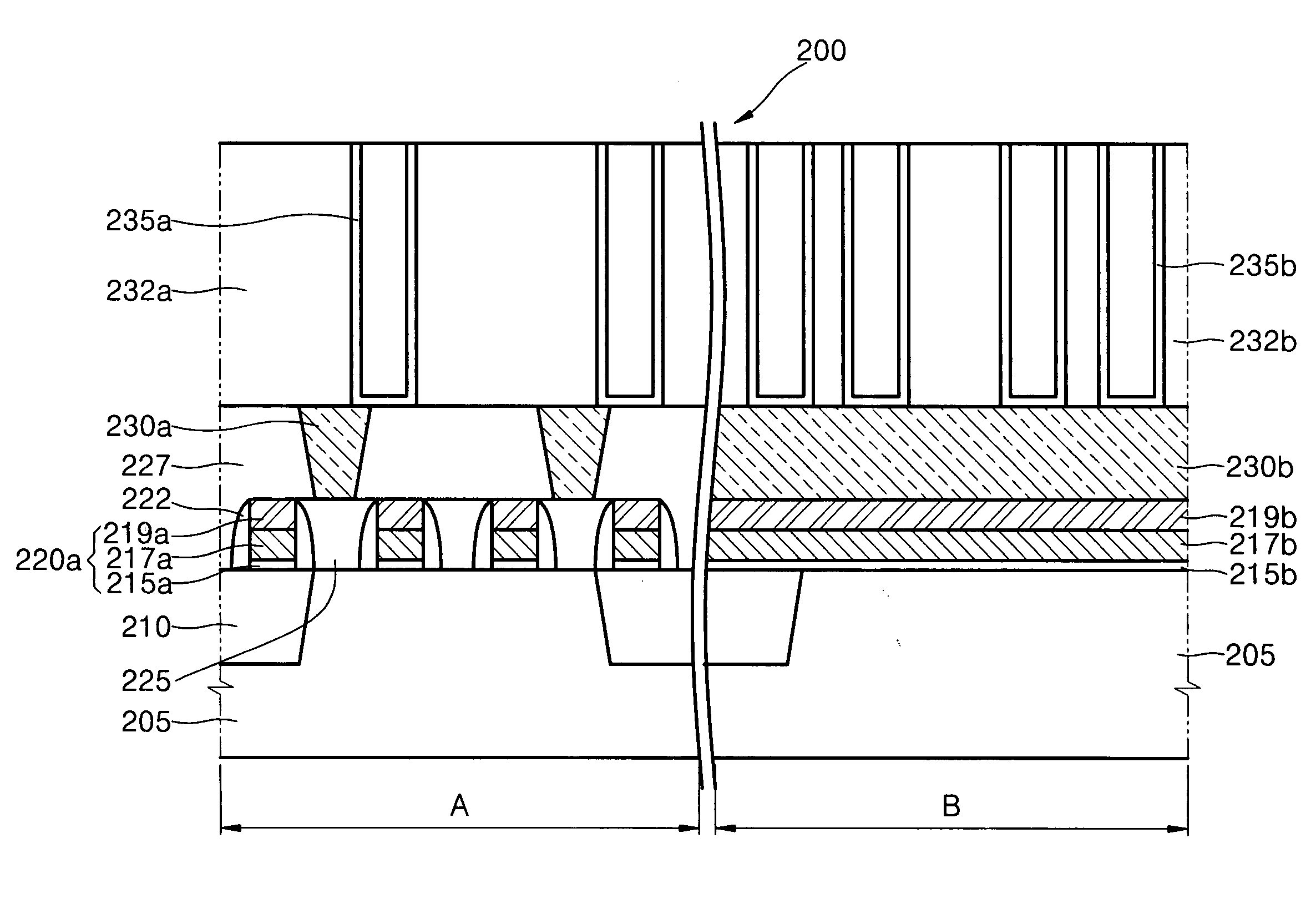
[0026] Exemplary embodiments of the present invention will now be described more fully hereinafter below with reference to the accompanying drawings. This invention may, however, be embodied in different forms and should not be construed as limited to the exemplary embodiments set forth herein. Rather, these exemplary embodiments are provided so that this disclosure will be through and complete, and will fully convey the scope of the invention to those skilled in the art. FIG. 3 is a cross-sectional view illustrating a semiconductor device according to an exemplary embodiment of the present invention. Referring to FIG. 3, a semiconductor memory device 200 has a cell region A and a decoupling capacitor region B. A cell capacitor of the cell region A includes storage nodes 235a and a decoupling capacitor includes storage nodes 235b. The two storage nodes 235a and 235b may be simultaneously formed in the same structure.

[0027] The storage nodes 235a and 235b are connected with the resp...


PUM


Abstract

A semiconductor memory device comprises a cell capacitor having a first buried contact connected with a semiconductor substrate of a cell region and a first storage node connected with the first buried contact, and a decoupling capacitor for reducing a coupling noise, having a plurality of second buried contacts formed on a semiconductor substrate portion adjacent in the cell region and extended in parallel with each other and a plurality of second storage nodes connected with the second buried contacts.

Description

CROSS-REFERENCE TO RELATED APPLICATION [0001] This application claims priority to Korean Patent Application No. 10-2004-0099051, filed on Nov. 30, 2004, the disclosure of which is incorporated herein in its entirety by reference. TECHNICAL FIELD [0002] The present disclosure relates to a semiconductor memory device, and more particularly, to a semiconductor memory device having a decoupling capacitor. BACKGROUND [0003] Semiconductor memory devices, e.g., dynamic random access memories (DRAMs), require high speed as well as high integration. A logic part such as a central processing unit (CPU) of semiconductor products becomes fast in its speed to process more data for a short time. Accordingly, an increase in speed as well as in a storage capacity of the semiconductor memory devices such as DRAMs becomes important. [0004] A speed increase of the semiconductor memory devices can be generally realized using a metal wiring having low resistance. For example, a copper wiring is used to ...

Claims


Application Information

Patent Timeline
IPC IPC(8): H01L29/00
CPCH01L27/0207H01L27/10855H01L27/10894H01L28/91H10B12/09H10B12/0335H10B99/00H10B12/00
Inventor PARK, JE-MINHWANG, YOO-SANG
Owner SAMSUNG ELECTRONICS CO LTD
Why Eureka
Try Eureka