Plasma display panel
- Summary
- Abstract
- Description
- Claims
- Application Information
AI Technical Summary
Benefits of technology
Problems solved by technology
Method used
Image
Examples
first exemplary embodiment
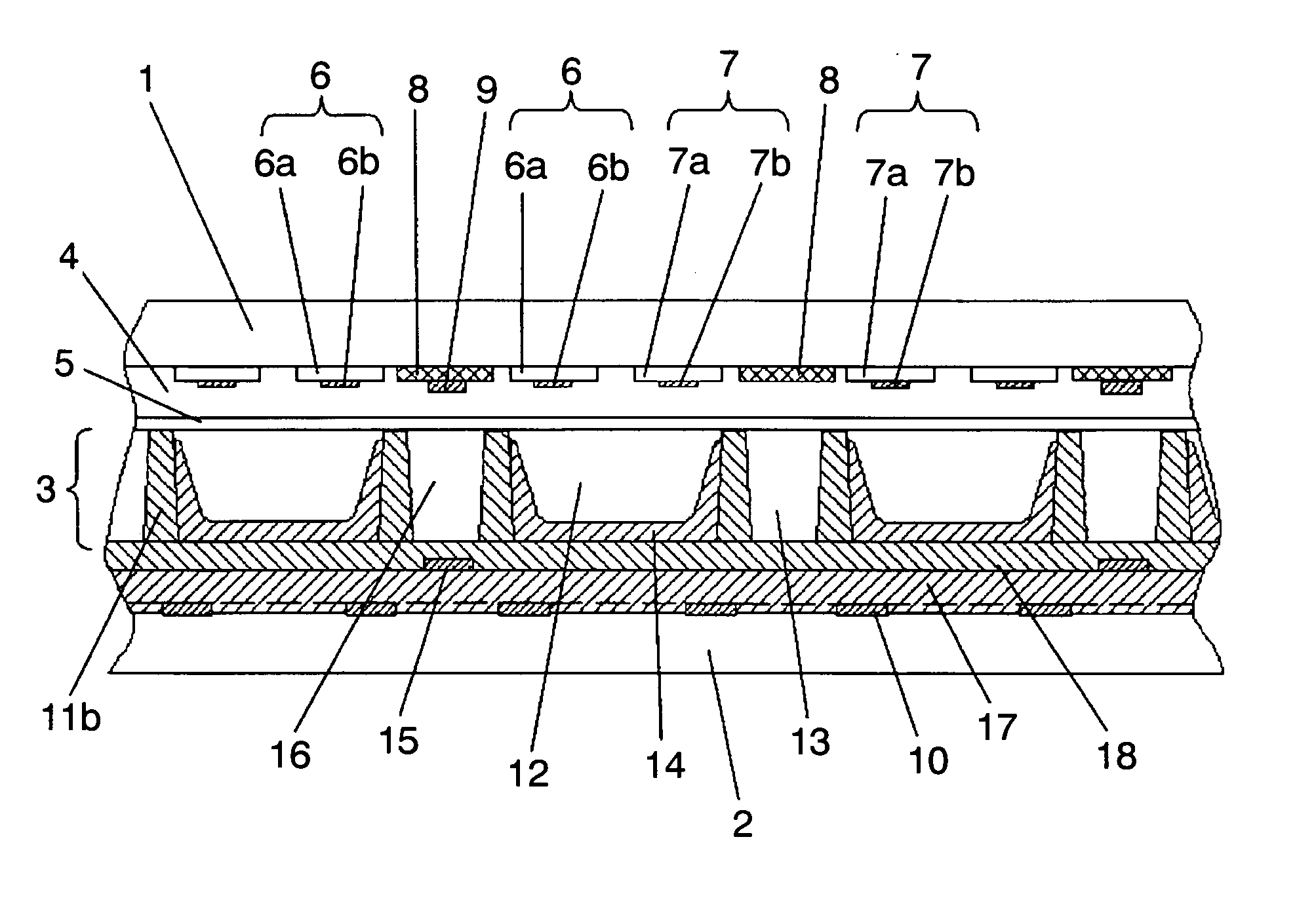
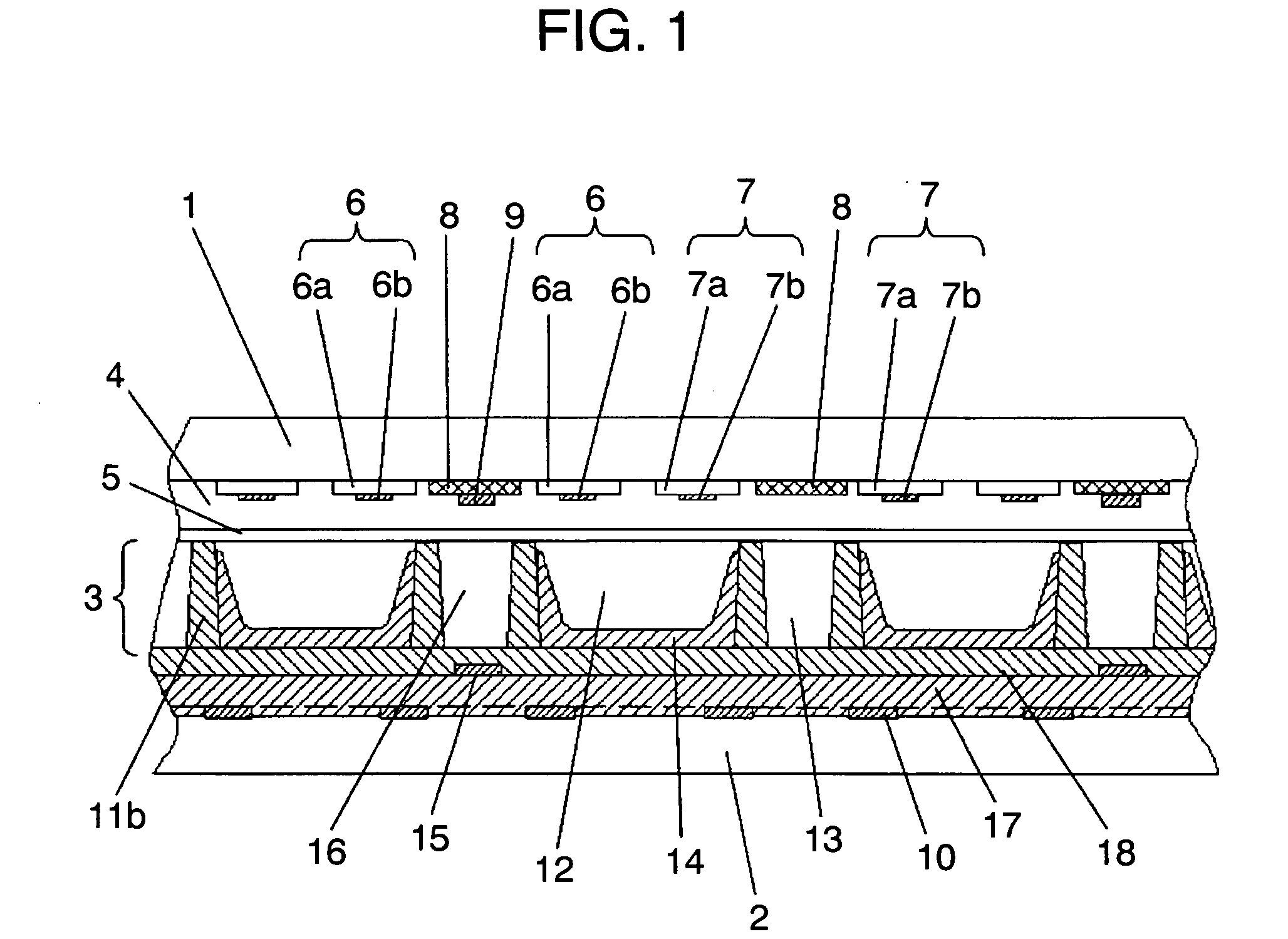
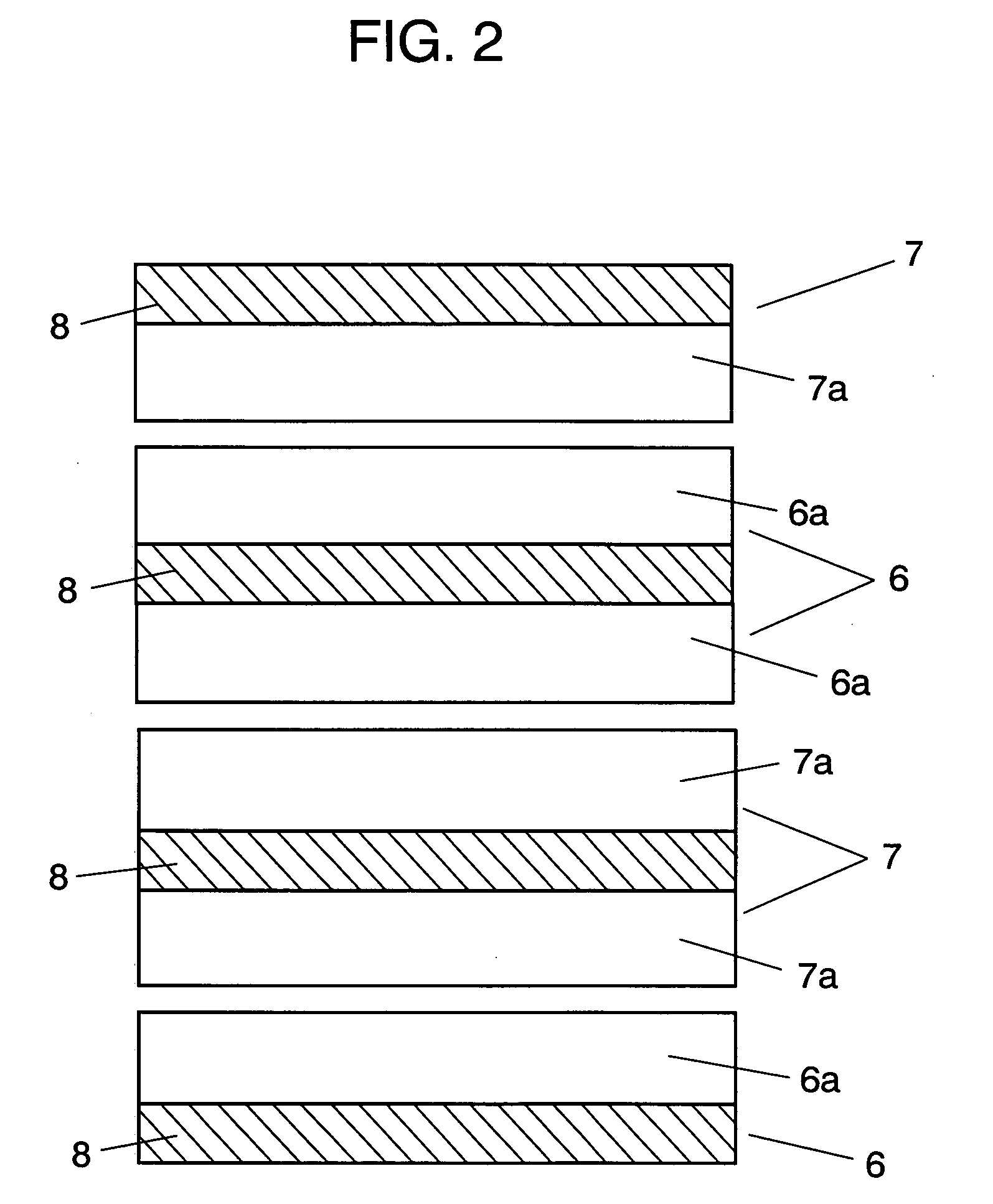
[0029]FIG. 1 is a sectional view showing a PDP in accordance with an exemplary embodiment of the present invention. FIG. 2 is a schematic plan view of an electrode array on the side of a front substrate as a first substrate. FIG. 3 is a schematic perspective view of the side of a back substrate as a second substrate.
[0030] As shown in FIG. 1, glass-made front substrate 1 as the first substrate and glass-made back substrate 2 as the second substrate are faced to each other through discharge space 3, neon (Ne) and xenon (Xe) as gas that emits ultraviolet rays by discharge are filled into discharge space 3. Band-like electrode groups are disposed in parallel on front substrate 1. Each of the electrode groups is covered with front substrate dielectric layer 4 and protective film 5 and has a pair of scan electrode 6 as a first electrode and sustain electrode 7 as a second electrode. Scan electrode 6 and sustain electrode 7 are formed of transparent electrodes 6a and 7a and metal buses 6...
second exemplary embodiment
[0046]FIG. 7 is a perspective view showing a shape of data electrode 10 in accordance with the second exemplary embodiment of the present invention. In the second exemplary embodiment, slotted parts 10a in data electrode 10 are circular or elliptic holes. The configuration except for slotted parts 10a is similar to that of embodiment 1.
[0047] Forming slotted parts 10a in data electrode 10 as the circular or elliptic holes produces the following advantage. In other words, though space for releasing the air bubble is narrower than that in the case using square holes, stress concentration can be suppressed because the holes of slotted parts 10a have no sharp edge, and torsion or chamber due to heating can be reduced. As a result, a PDP having high reliable and no cause of dielectric breakdown in addition to the advantage described in embodiment 1 can be realized.
third exemplary embodiment
[0048]FIG. 8 is a perspective view showing a shape of data electrode 10 in accordance with the third exemplary embodiment of the present invention. In the third exemplary embodiment, slotted parts 10a in data electrode 10 have a shape where side parts are alternately notched in the longitudinal direction of data electrode 10. The configuration except for slotted parts 10a is similar to that of embodiment 1. Forming slotted parts 10a in this shape allows the hole area, namely the space for releasing the air bubble, to be enlarged, and largely suppresses the deformation of data electrode 10 due to the air bubble. A PDP having high reliable and no cause of dielectric breakdown can be realized.
[0049] In the manufacturing processes of exemplary embodiments 1 to 3 of the present invention, data electrodes 10, first dielectric layer 17, priming electrodes 15, second dielectric layer 18, barrier ribs 11, and phosphor layers 14 are sequentially applied, burned, and solidified. However, for ...
PUM
 Abstract
Description
Claims
Application Information


