Method for manufacturing printed wiring board

a printing method and wiring board technology, applied in the direction of printed circuit assembling, resistive material coating, non-metallic protective coating application, etc., can solve the problems of air bubbles, air voids to be produced air in the resin layer, etc., to facilitate the spreading of resin, easy to remove, and easy to polish

Active Publication Date: 2006-06-01
NODA SCREEN
View PDF2 Cites 6 Cited by
  • Summary
  • Abstract
  • Description
  • Claims
  • Application Information

AI Technical Summary

Benefits of technology

[0014] By performing the above described steps in order, it is possible to obtain a flat substrate in which only a very thin resin layer remains on the circuit patterns. Additionally, a flat substrate is obtained in which the spaces between the circuit patterns are filled with a resin layer containing hardly any air bubbles. Then, by polishing the substrate so as to not damage the circuit pattern, the extremely thin resin layer can be easily removed, obtaining a smooth substrate with exposed circuit patterns.
[0015] When the smoothing plate is pressed against a resin layer located on the substrate, a metallic foil with a roughened surface facing the resin layer, which metallic foil is interposed between the smoothing plate and the resin layer, facilitates the spreading of the resin. The metallic foil also forms the surface of the resin layer in a fine uneven state in accordance with the roughened surface of the metallic foil. As a result, the residual resin layer can be more easily polished.
[0016] Further, in the case where the metallic foil interposed between the smoothing plate and the resin layer is formed of a different type of metal from the circuit patterns, it is possible to remove the metallic foil by selective etching or dissolving only the metallic foil without affecting the metal of the circuit patterns.

Problems solved by technology

However, the circuit pattern of a printed board, which is manufactured via a subtractive method of removing unnecessary parts of copper foil through etching, is generally formed into an uneven state in which the circuit pattern is raised from the surface of the base material.
However, the method of applying a resin via screen printing has a problem in that air is inevitably involved with the resin during the printing.
The involved air results in minute air bubbles, causing voids to be produced in the resin layer.
The method of laminating a resin sheet also has a problem that air enters between the resin sheet and the substrate and results in air bubbles.
This also causes voids to be produced in the resin layer.
Such voids are not preferred because they tend to burst during the heating stage of a subsequent process, or the voids may deteriorate the electrical characteristics of the substrate.
On the other hand, however, there is a problem that a resin with a lowered viscosity can flow out from the spaces between the circuit patterns when the resin layer is pressed.

Method used


Image

  • Method for manufacturing printed wiring board
  • Method for manufacturing printed wiring board
  • Method for manufacturing printed wiring board

Examples


Embodiment Construction

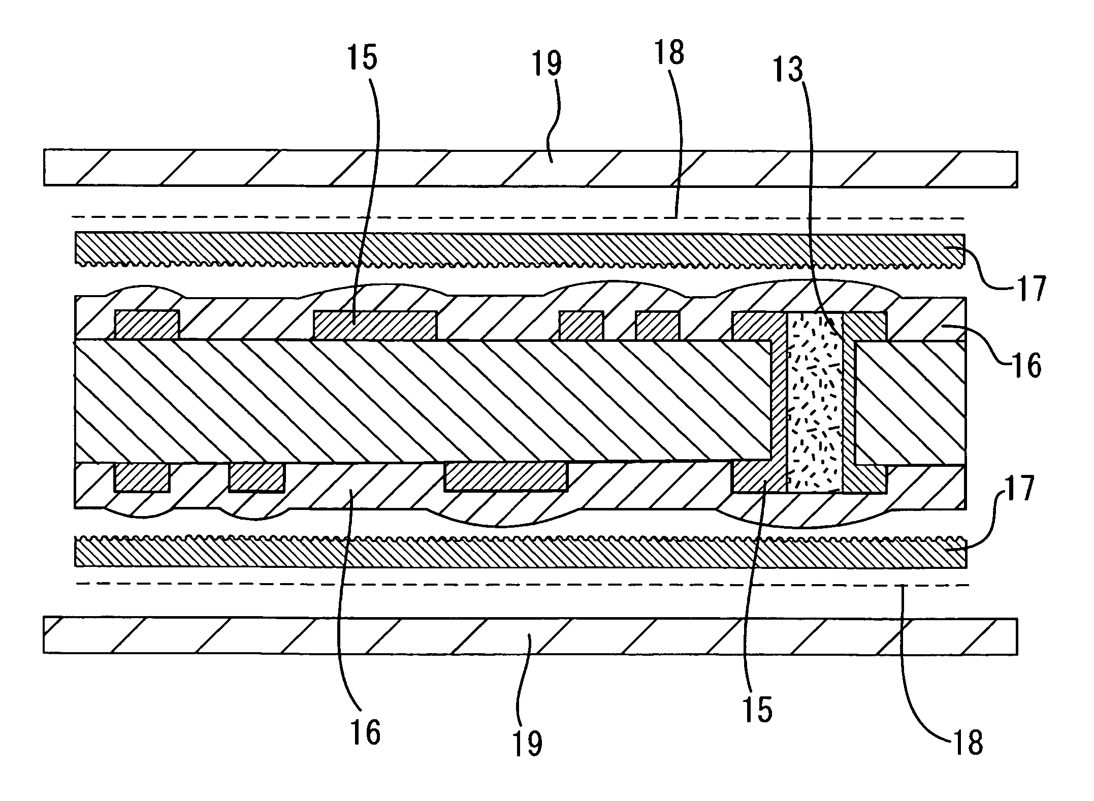
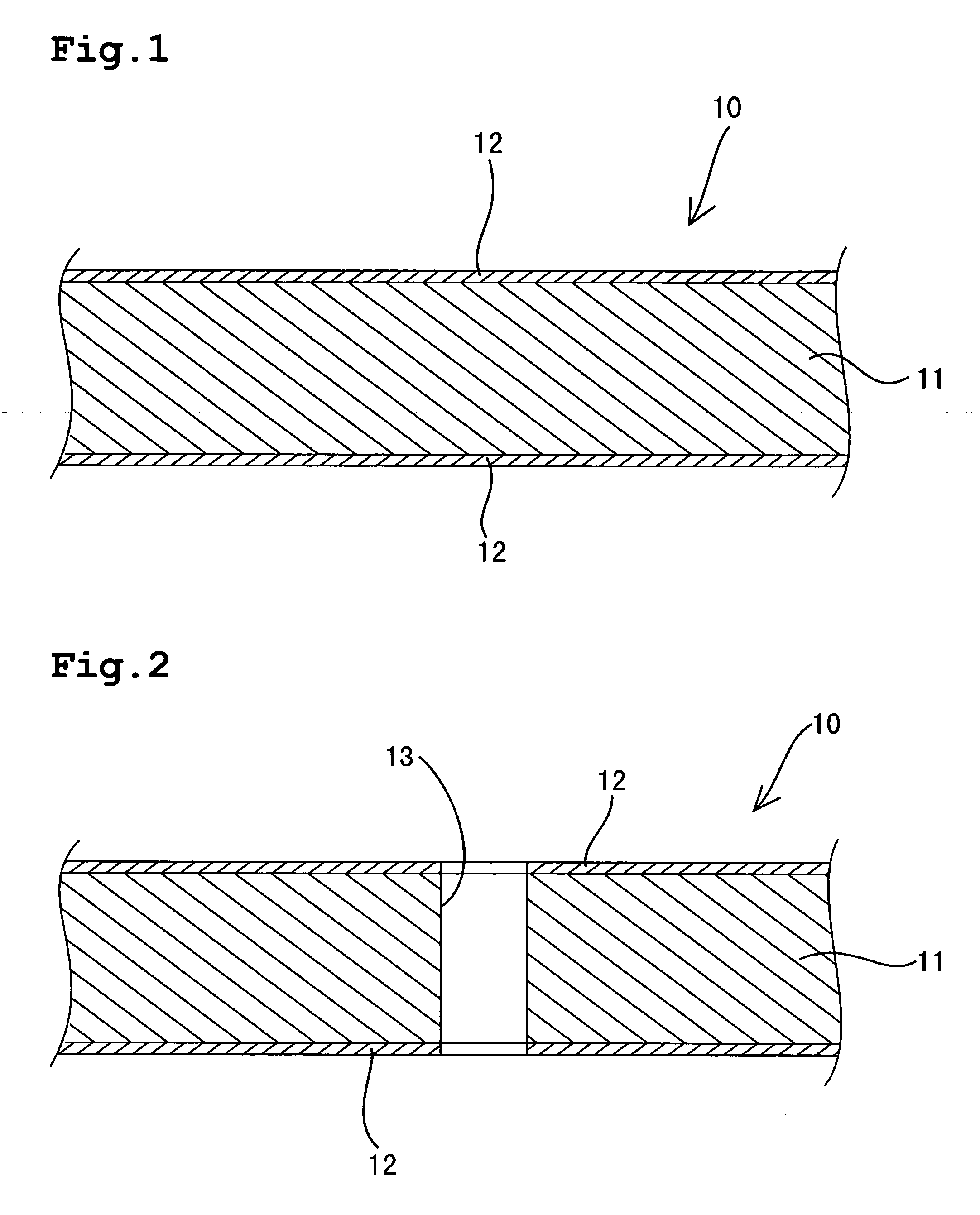
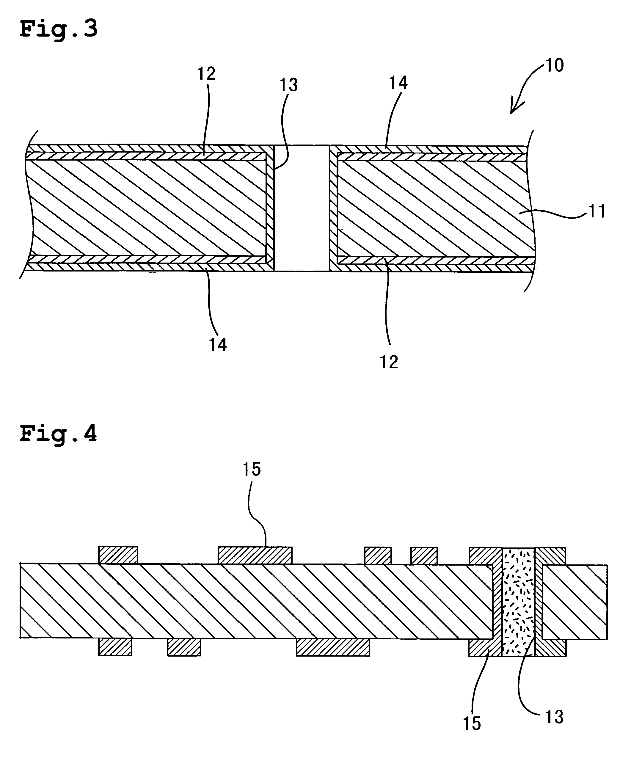
[0027] In the present embodiment, as shown in FIG. 1, a copper clad laminated board 10 with copper foils 12 adhered to both sides of a glass epoxy substrate 11 having a thickness of 100 to 3,000 μm is used as a base material. Boring through the copper clad laminated board 10 at required positions forms the through holes 13 (see FIG. 2). Chemical plating and electrolytic plating are performed in order to form the copper plated layers 14 upon the entire surface area, including the inner peripheral face of the through holes 13, so as to make the thickness of the conductor layer on the surface of the substrate approach approximately 20 μm (see FIG. 3). A resin then fills in the through holes 13 and is cured. Polishing flattens the resin projected to the surface of the substrate. Circuit patterns 15 are then formed on the smoothed substrate by a known photo-etching method (see FIG. 4).

[0028] As shown in FIG. 5, a liquid thermosetting epoxy resin is then applied to the wiring board by e....


PUM

PropertyMeasurementUnit
temperatureaaaaaaaaaa
thicknessaaaaaaaaaa
thicknessaaaaaaaaaa

Abstract

A method for manufacturing a printed wiring board, including the steps of: forming a thermosetting resin layer so as to fill the spaces between circuit patterns formed on the printed wiring board; heating and curing the resin layer in a reduced pressure chamber in which the pressure is reduced while a smoothing plate is pressed against the resin layer; and then polishing the cured resin layer covering the circuit patterns, thereby exposing the circuit patterns. The step of heating and curing the resin layer in the reduced pressure chamber comprises the following successively performed steps: step 1: maintaining the resin layer at a non-curable temperature to prevent the resin layer from curing, in a state where the resin layer is pressed via the smoothing plate in the reduced pressure chamber; step 2: heating the resin layer in the pressed state to a curing temperature at which the resin layer is cured; step 3: introducing outside air into the reduced pressure chamber with the pressed state and the curing temperature maintained; step 4: reducing the pressure applied to the smoothing plate with the curing temperature maintained; and step 5: cooling the resin layer.

Description

TECHNICAL FIELD [0001] The present invention relates to a method for manufacturing a printed wiring board. BACKGROUND ART [0002] In the case of manufacturing a multilayer printed wiring board by e.g. a build-up method, it is necessary to flatten the surface of a lower layer substrate in order to increase the wiring density. However, the circuit pattern of a printed board, which is manufactured via a subtractive method of removing unnecessary parts of copper foil through etching, is generally formed into an uneven state in which the circuit pattern is raised from the surface of the base material. [0003] Thus, a method has been proposed in order to flatten the printed board, of which the surface is formed in such an uneven form, in which a thermosetting resin is filled into the spaces between the circuit patterns and cured by heating. The surface of the resin is then polished. [0004] The above described method for filling the spaces between circuit patterns with a resin includes for e...

Claims


Application Information

Patent Timeline
Patent Type & Authority Applications(United States)
IPC IPC(8): B05D5/12B05D3/00B05D3/02B05D3/12H05K3/22H05K3/28H05K3/46
CPCH05K3/28H05K2201/09881H05K2203/025H05K2203/0278H05K2203/085Y10T29/49126H05K2203/1476Y10T29/49156Y10T29/49128Y10T29/49155H05K2203/1152H05K3/22H05K3/46
Inventor MURAKAMI, KEIICHI
Owner NODA SCREEN
Why Eureka
Try Eureka