PLL circuit

a circuit and circuit technology, applied in the direction of electrical equipment, pulse automatic control, etc., can solve the problems of reducing affecting the speed of the system, and taking a long time to produce a stable frequency, so as to reduce the power consumption of the system, the effect of simple structur

Inactive Publication Date: 2006-06-08
SHARP KK
View PDF8 Cites 21 Cited by
  • Summary
  • Abstract
  • Description
  • Claims
  • Application Information

AI Technical Summary

Benefits of technology

[0021] The present invention, conceived in view of the aforementioned conventional problems, has an objective to realize a PLL circuit which with a simple structure increases the speed of and reducing the power consumption of a system which are frequently and repeatedly turned on / off, such as a wireless LAN system.

Problems solved by technology

The PLL circuit and associated circuitry consume a lot of power.
The PLL circuit however has a problem that it takes time to produce a stable frequency after the power supply is turned on.
Nevertheless, the standby period still accounts for a large portion of the entire packet cycle.
The structure may present an obstacle to reduction of power consumption, especially if it is employed in a system whose power supply is frequently turned on / off.
This may lead to increase in IC chip size and power consumption.

Method used


Image

  • PLL circuit
  • PLL circuit
  • PLL circuit

Examples


example 1

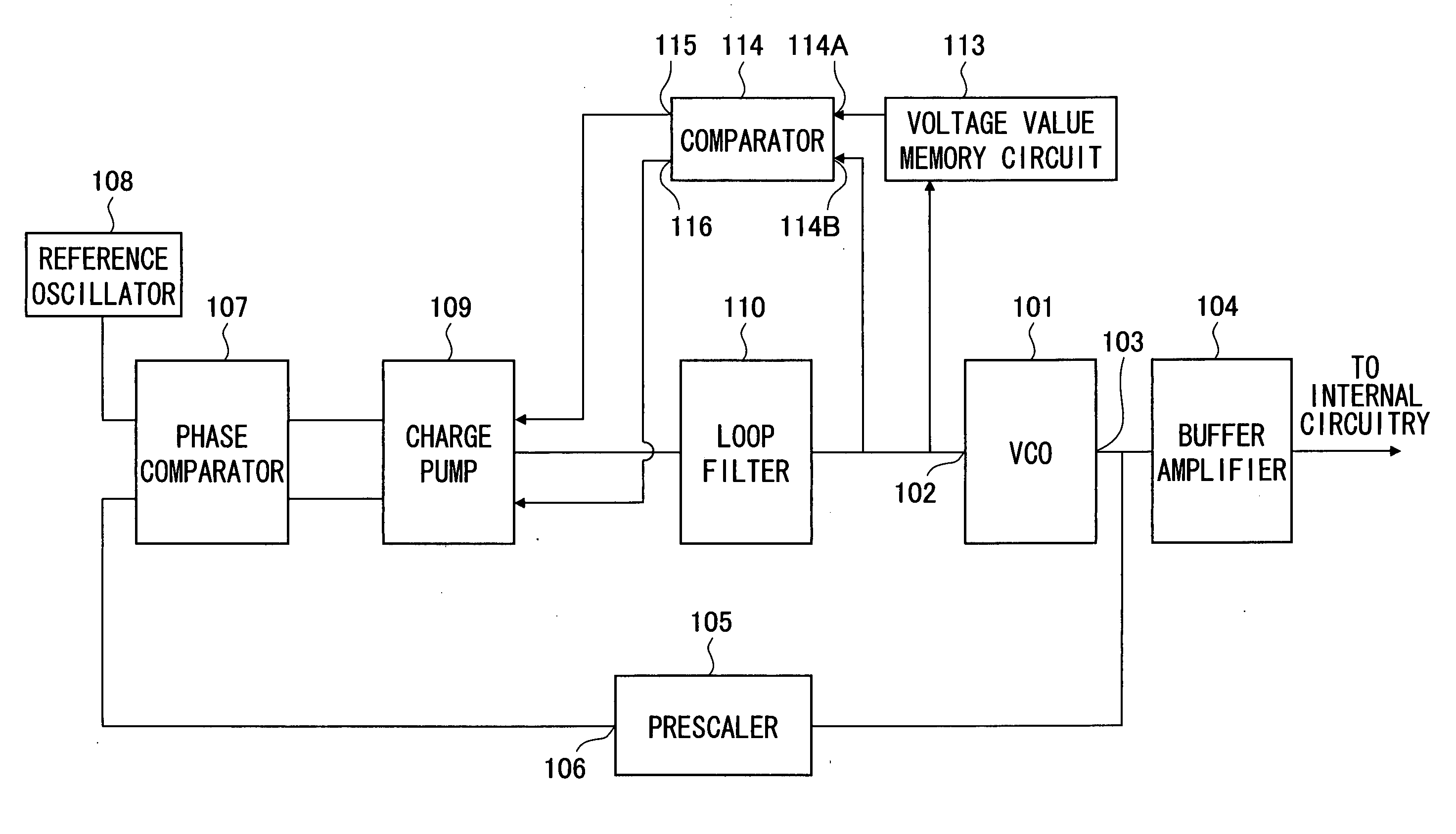
[0061]FIG. 2 is a block diagram illustrating the structure of a PLL circuit which represents example 1 of the present invention. As shown in the figure, The PLL circuit of the present example includes a circuit containing a switch 213A and a capacitor 213B as the voltage value memory circuit 213. The capacitor 213B is located at a position equivalent to that of the capacitor 211 in the loop filter 210. The capacitor 213B is therefore a part of the loop filter 210 while the PLL is in operation.

[0062] Whether the phase difference signal or the comparison signal is fed to the charge pump 209 is controlled in accordance with whether the PLL circuit is in a normal operation mode (ON) or in a standby mode (OFF). Thus there are provided AND circuits 217, 218, 219, 220 to the phase difference signal output of the phase comparator 107 and the comparison signal output of the comparator 114. In addition, in the PLL circuit of the present example the charge pump 209 is constructed of: a source...

example 2

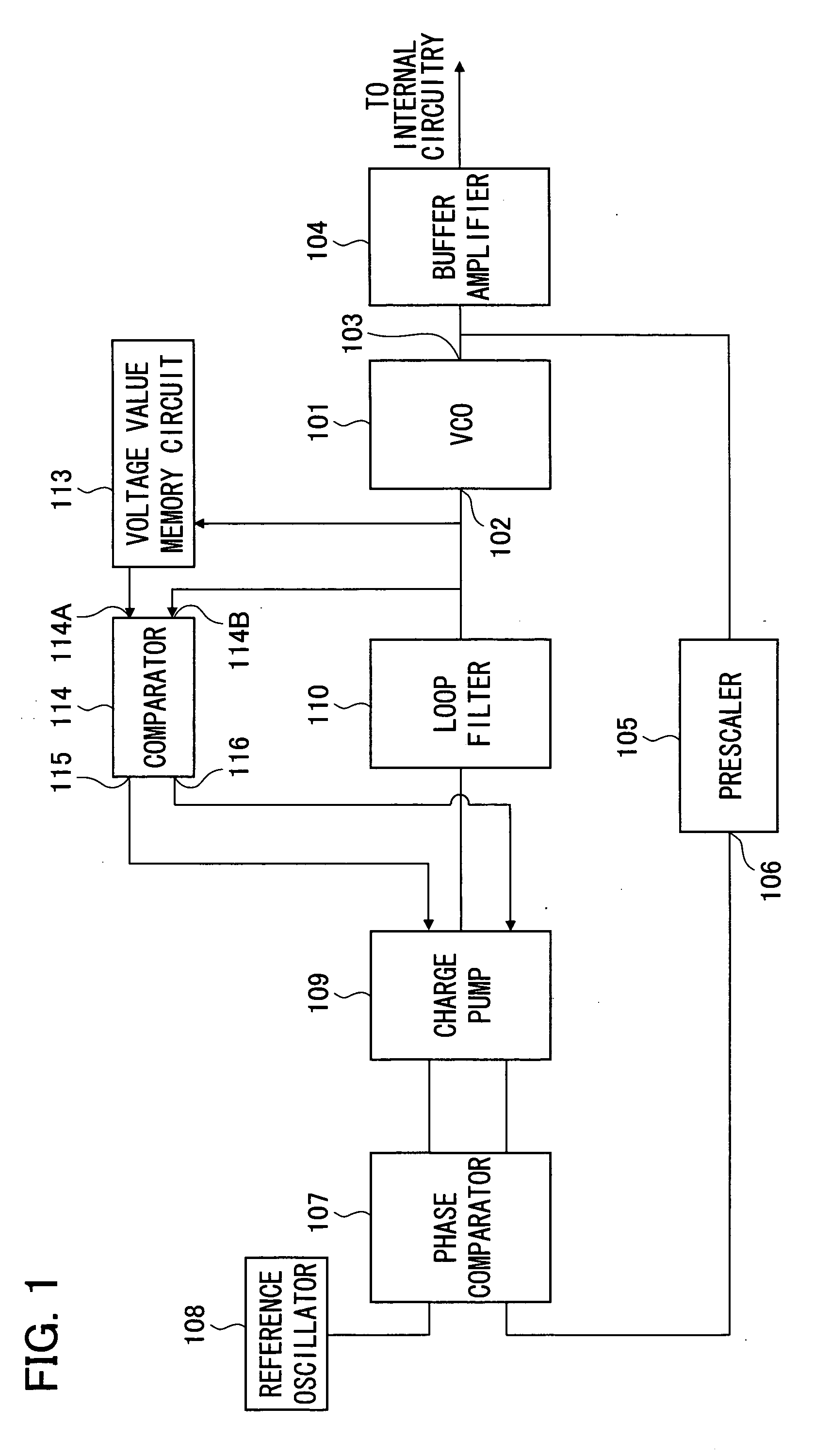
[0067]FIG. 3 is a block diagram illustrating the structure of a PLL circuit which represents example 2 of the present invention. As shown in the figure, the present example differs from example 1 above in the voltage value memory circuit 313; otherwise, example 2 has the same structure as example 1.

[0068] The voltage value memory circuit 313 of the present example includes an A / D converter 327, a D / A converter 328, and a memory 329. The A / D converter 327 is connected to the loop filter 210 and the memory 329. The A / D converter 327 converts an analog signal input of the loop filter 210 to digital for an output to the memory 329 where the output is recorded. The D / A converter 328 is connected to the memory 329 and the comparator 114. The D / A converter 328 converts a digital signal stored in the memory 329 to an analog signal for an output to the comparator 114.

[0069] The voltage value memory circuit 313 operates in the same fashion as the voltage value memory circuit 113 (see FIG. 1...

example 3

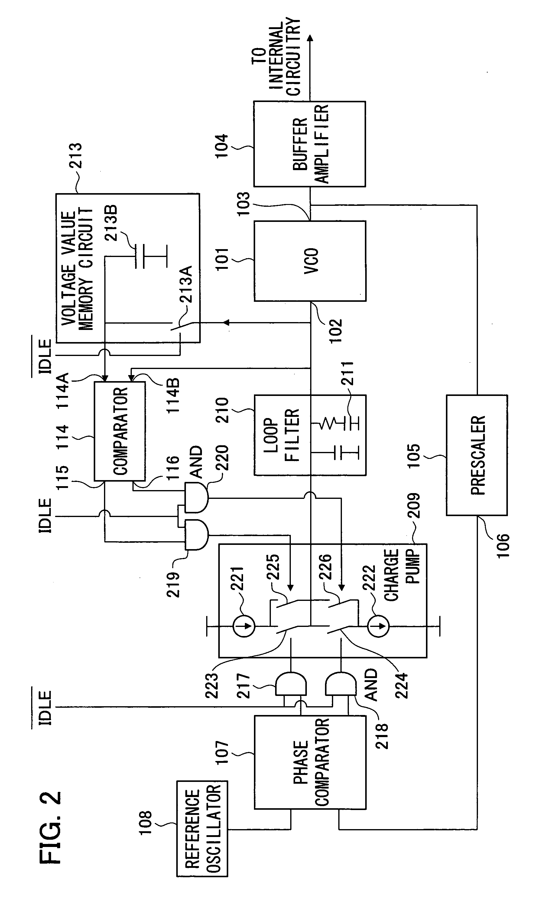
[0071]FIG. 4 is a block diagram illustrating the structure in and around a charge pump of a PLL circuit which represents example 3 of the present invention. As shown in the figure, in the present example, the output signals of the phase comparator and the comparator are coupled using a multiplexer, which reduces the number of current control switches for the charge pump as compared to examples 1, 2. The PLL circuit of the present example differs from those of examples 1, 2 in that the charge pump has less internal current control switches than in examples 1, 2 and that the output signals of the phase comparator and the comparator are coupled using a multiplexer; otherwise, the present example has the same structure as examples 1, 2.

[0072] The charge pump 409 in the PLL circuit of the present example is constructed of a source power supply, or current supplier, 421; a sink power supply, or current drawer, 422; and switches 423, 424 which are turned on / off by a signal from either the...


PUM


Abstract

The PLL circuit of the present invention includes a voltage-controlled oscillator, a loop filter, and a charge pump which controls a voltage of the loop filter while the voltage-controlled oscillator is not oscillating. Therefore, it is possible, even while the voltage-controlled oscillator is not oscillating, to control a voltage for the charge pump so that it is equal to a voltage when the voltage-controlled oscillator is oscillating at a predetermined frequency. Accordingly, by the loop filter outputting a voltage signal to the voltage-controlled oscillator when the PLL circuit is turned on, the pull-in time can be shortened.

Description

[0001] This nonprovisional application claims priority under 35 U.S.C. § 119(a) on Patent Application No. 2004-350472 filed in Japan on Dec. 2, 2004, the entire contents of which are hereby incorporated by reference. FIELD OF THE INVENTION [0002] The present invention relates to PLL circuits used for the purpose of increasing the speed of and reducing the power consumption of a system which frequently and repeatedly switches on / off, such as a wireless LAN system. BACKGROUND OF THE INVENTION [0003] Apparatus, such as mobile phones and wireless LAN systems, includes a PLL circuit so that the oscillator section can produce a high frequency signal. The PLL circuit and associated circuitry consume a lot of power. To reduce power consumption in such apparatus, the PLL circuit is activated only when necessary, for example, in transmission and reception. That is, the PLL circuit is frequently turned on / off. A conventional, popular approach to reduce power consumption in mobile phones, wirel...

Claims


Application Information

Patent Timeline
Patent Type & Authority Applications(United States)
IPC IPC(8): H03L7/00
CPCH03L7/0802H03L7/0891H03L7/10H03L7/18H03L7/1075H03L7/093
Inventor ISOBE, MASAYAADAN, ALBERT O.
Owner SHARP KK
Why Eureka
Try Eureka