System and method for optimizing printed circuit boards to minimize effects of non-uniform dielectric

a technology of non-uniform dielectric properties and optimizing printed circuit boards, which is applied in the field of computer systems, can solve problems such as problems such as problems such as problems such as uneven dielectric constants of materials used to manufacture pcbs, and problems such as signal propagation delay variations, and achieve the effect of improving dielectric property uniformity

Active Publication Date: 2006-06-08
DELL PROD LP
View PDF16 Cites 24 Cited by
  • Summary
  • Abstract
  • Description
  • Claims
  • Application Information

AI Technical Summary

Benefits of technology

[0010] The present disclosure includes a number of important technical advantages. One technical advantage is forming a first and second trace on a printed circuit board in a third direction which is offset from the directions corresponding to the fibe

Problems solved by technology

The dielectric constant of the materials used to manufacture PCBs is not uniform.
This difference in dielectric constant often causes variations in the signal propagation delay due to the positioning of the traces formed on the PCB relative to the glass fiber.
This variation in signal propagation delay is problematic when more than one trace (such as a differential pair) are used to transfer data from a transmitter module to a receiver module, because

Method used


Image

  • System and method for optimizing printed circuit boards to minimize effects of non-uniform dielectric
  • System and method for optimizing printed circuit boards to minimize effects of non-uniform dielectric
  • System and method for optimizing printed circuit boards to minimize effects of non-uniform dielectric

Examples


Embodiment Construction

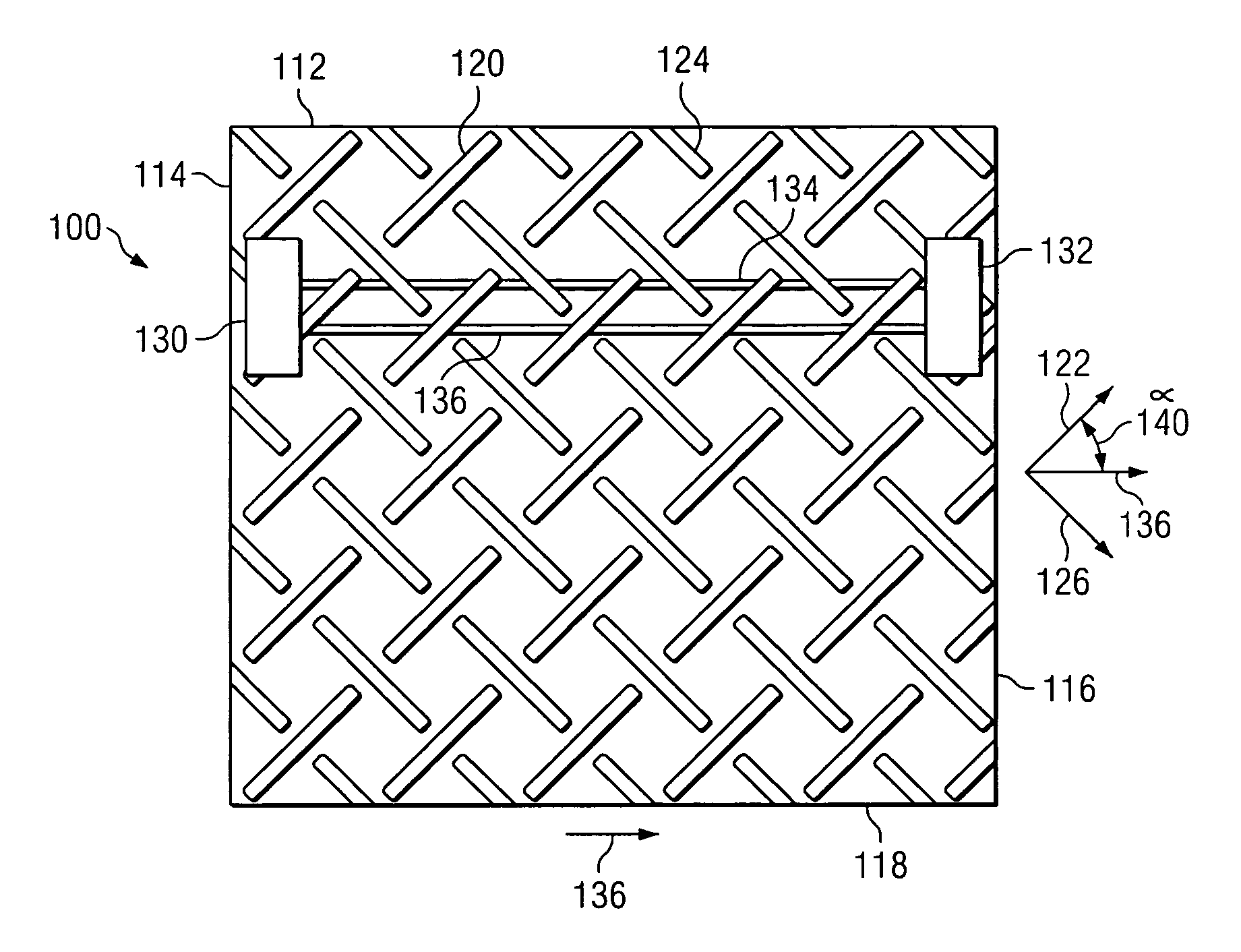
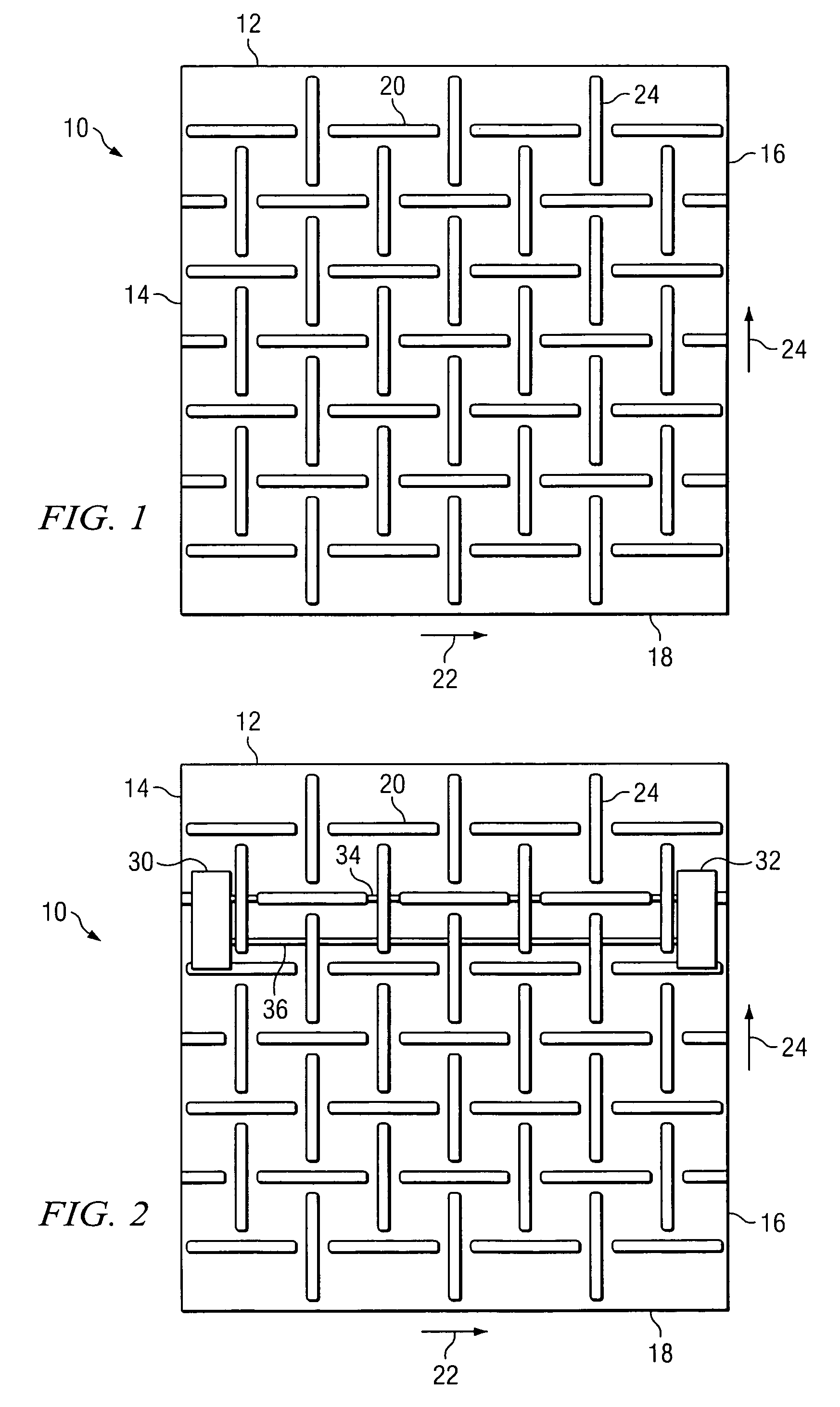
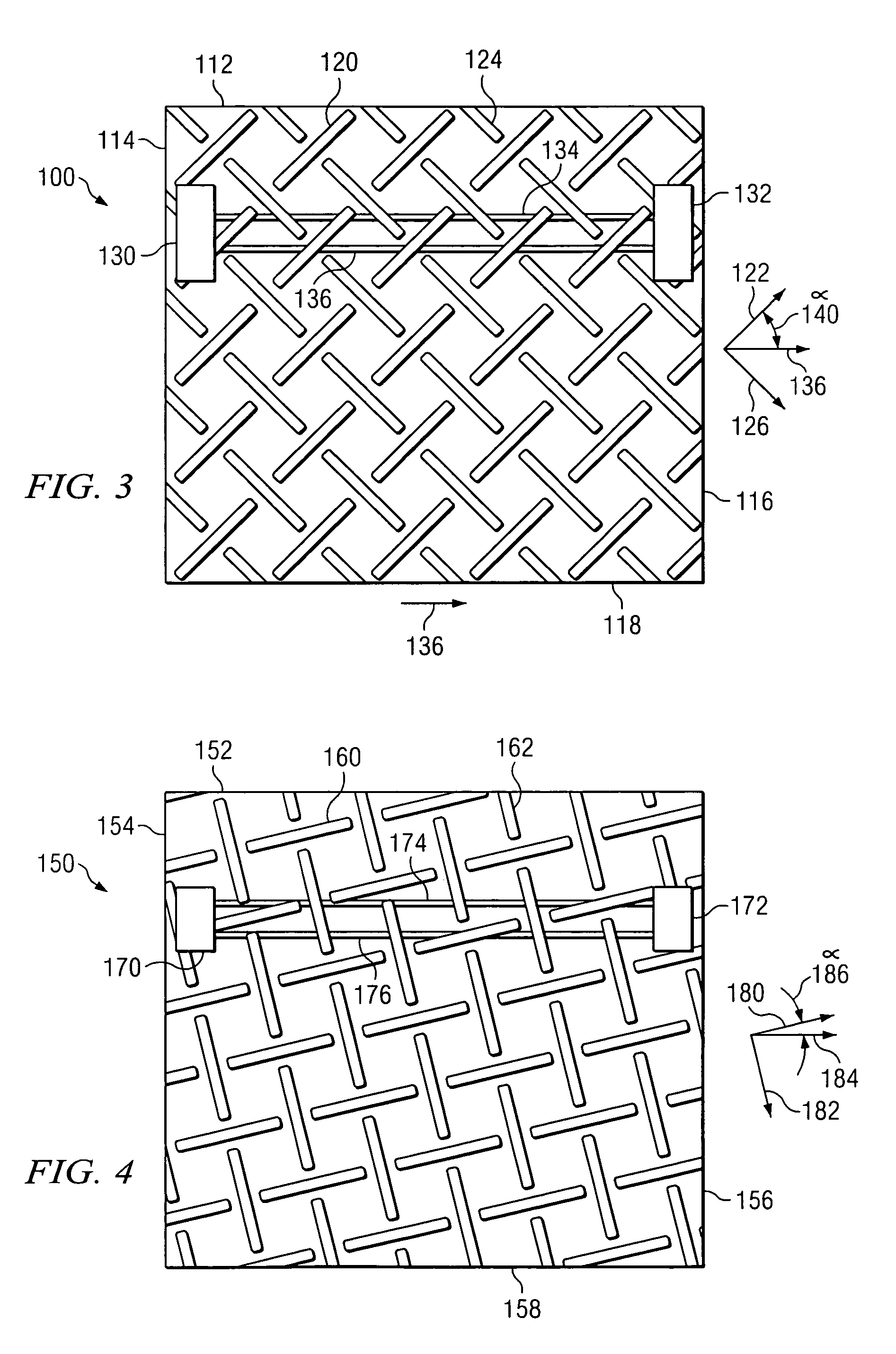
[0017] Preferred embodiments of the invention and its advantages are best understood by reference to FIGS. 1-9 wherein like numbers refer to like and corresponding parts.

[0018] As the value and use of information continues to increase, individuals and businesses seek additional ways to process and store information. One option available to users is information handling systems. An information handling system generally processes, compiles, stores, and / or communicates information or data for business, personal, or other purposes thereby allowing users to take advantage of the value of the information. Because technology and information handling needs and requirements vary between different users or applications, information handling systems may also vary regarding what information is handled, how the information is handled, how much information is processed, stored, or communicated, and how quickly and efficiently the information may be processed, stored, or communicated. The variati...


PUM

PropertyMeasurementUnit
Angleaaaaaaaaaa
Angleaaaaaaaaaa
Angleaaaaaaaaaa

Abstract

A system and method for minimizing the effects of non-uniform dielectric properties includes forming traces on printed circuit boards (PCB) where the fibers within the printed circuit boards are non-rectangular with respect to the rectangular edges of the circuit board. The orientation of the traces with respect to the fibers substantially minimizes the effects of non-uniform dielectric properties of the PCB.

Description

TECHNICAL FIELD [0001] The present invention is related to the field of computer systems and more specifically to a system and method for optimizing printed circuit board materials to minimize the effects of non-uniform dielectric properties. BACKGROUND OF THE INVENTION [0002] As the value and use of information continues to increase, individuals and businesses seek additional ways to process and store information. One option available to users is information handling systems. An information handling system generally processes, compiles, stores, and / or communicates information or data for business, personal, or other purposes thereby allowing users to take advantage of the value of the information. Because technology and information handling needs and requirements vary between different users or applications, information handling systems may also vary regarding what information is handled, how the information is handled, how much information is processed, stored, or communicated, an...

Claims


Application Information

Patent Timeline
IPC IPC(8): H05K7/06
CPCH05K1/0213H05K1/0366H05K2201/029H05K2201/09227H05K2201/09236
Inventor FARKAS, SANDOR TIBORPIKE, JIMMY D.
Owner DELL PROD LP
Why Eureka
Try Eureka