Method of fabricating CMOS image sensor

a technology of image sensor and cmos, which is applied in the field of image sensor, can solve the problems of abnormal device operation, reduced light condensing efficiency, and less than optimal light condensing efficiency, and achieve the effects of curvature of microlens, facilitating reflow of microlens, and raising the light condensing efficiency of microlens

Active Publication Date: 2006-06-15
III HLDG 4
View PDF2 Cites 18 Cited by
  • Summary
  • Abstract
  • Description
  • Claims
  • Application Information

AI Technical Summary

Benefits of technology

[0017] An object of the present invention is to provide a method of fabricating a CMOS image sensor, in which a trapezoid microlens pattern profile is formed to facilitate a reflow of a microlens and by which a curvature of the microlens may be enhanced to raise the light-condensing efficiency of the microlens.

Problems solved by technology

Since the pattern forming condition can be relatively unstable, the light-condensing efficiency can be less than optimal.
However, the convex microlens in the related art CMOS image sensor has the following problems.
Yet, light that is not parallel to the optical axis may be refracted by the lens and arrive at another photosensitive device that is not supposed to receive the light.
Hence, the device may operate abnormally.
Secondly, since a quantity of light arriving at the photosensitive device varies according to the species and thickness of the layer under the microlens, the light-condensing efficiency may be reduced and degrade the quality of the image.

Method used


Image

  • Method of fabricating CMOS image sensor
  • Method of fabricating CMOS image sensor
  • Method of fabricating CMOS image sensor

Examples


Embodiment Construction

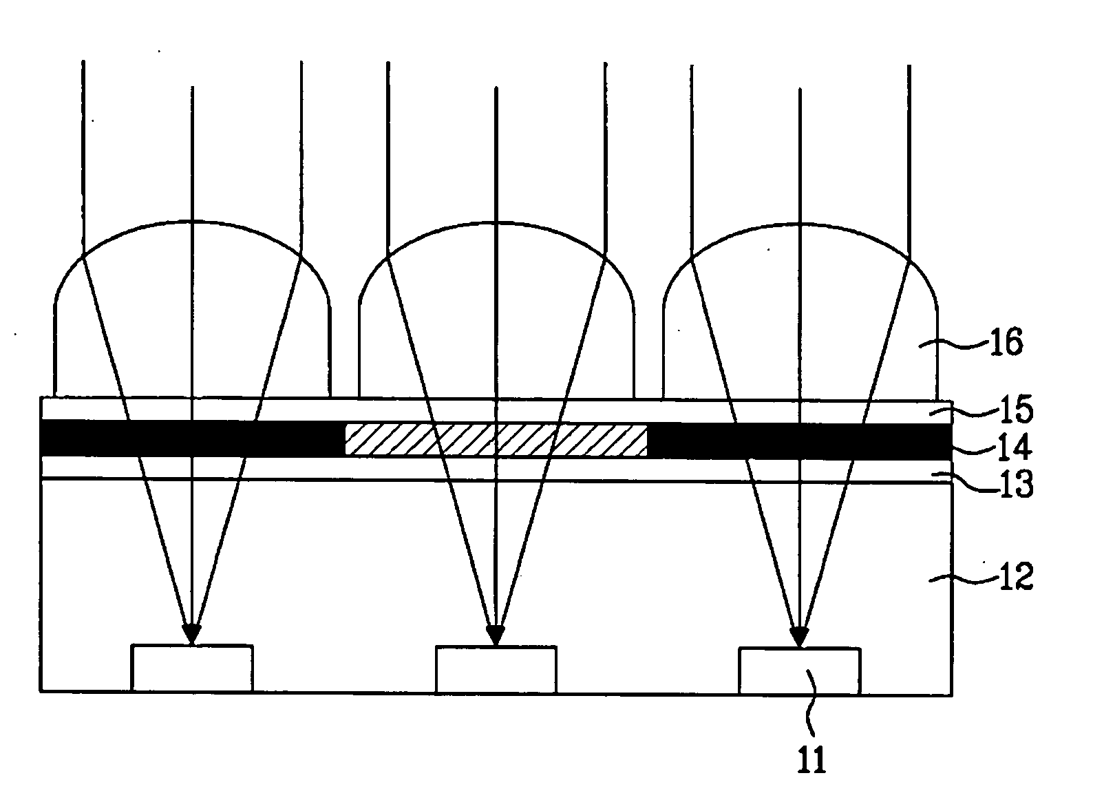
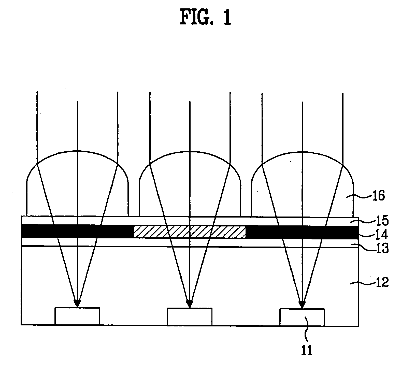
[0027] Reference will now be made in detail to the preferred embodiments of the present invention, examples of which are illustrated in the accompanying drawings. Wherever possible, like reference designations will be used throughout the drawings to refer to the same or similar parts.

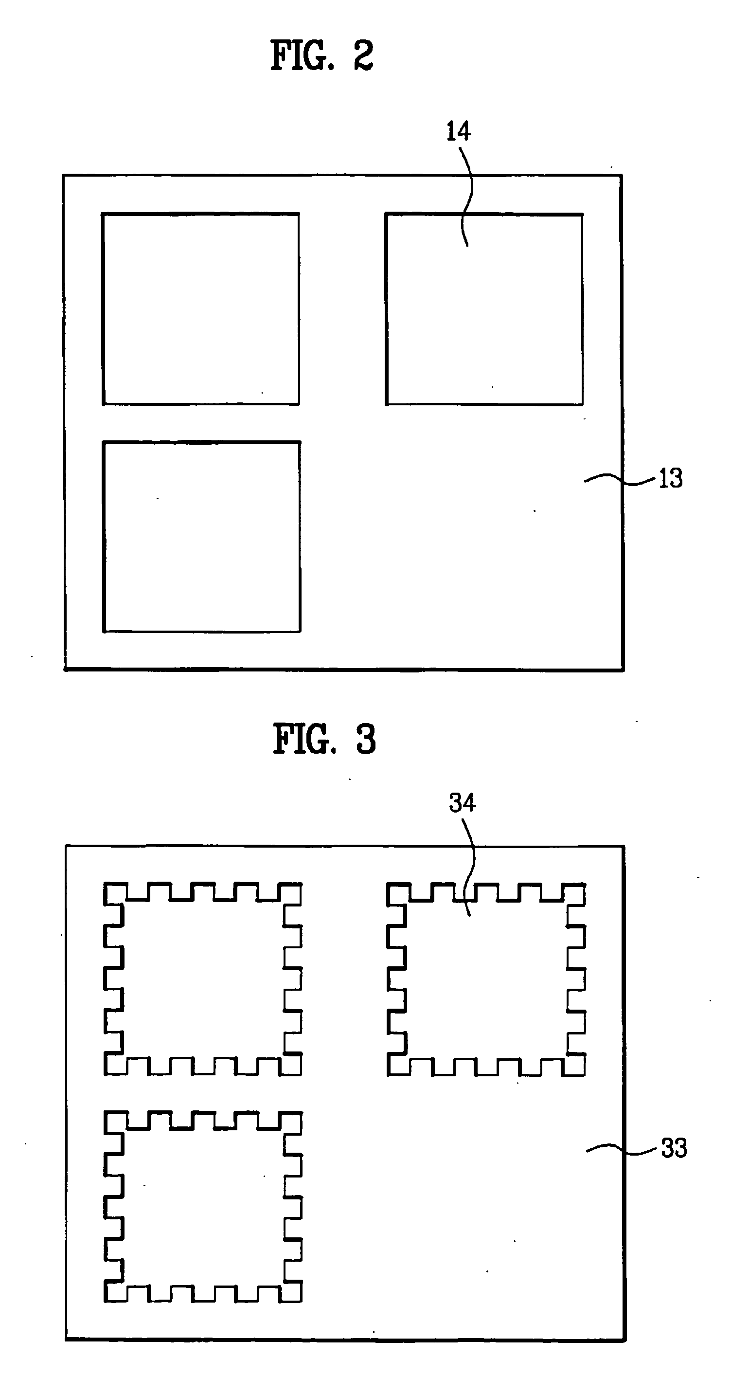
[0028]FIG. 3 shows a color filter layer on an insulating interlayer in a CMOS image sensor according to the present invention. Here, a plurality of color filter layers 34 are formed on an insulating interlayer 33, uniformly spaced apart from each other. The spacing in one dimension (e.g., along a first axis in the plane of the page parallel with an edge of the color filter) may be independent of the spacing in another dimension (e.g., along a second axis in the plane of the page, perpendicular to the first axis). In this case, a boundary or edge of each of the color filter layers 34 is indented or “stepped.” Also, the insulating interlayer 33 may further comprise a protective and / or planarizing layer a...


PUM


Abstract

A method of fabricating a CMOS image sensor is provided, in which a trapezoidal microlens pattern profile is formed to facilitate reflowing the microlens pattern and by which a curvature of the microlens may be enhanced to raise its light-condensing efficiency. The method includes forming a plurality of photodiodes on a semiconductor substrate; forming an insulating interlayer on the semiconductor substrate including the photodiodes; forming a protective layer on the insulating interlayer; forming a plurality of color filters corresponding to the photodiodes; forming a top coating layer on the color filters; forming a microlens pattern on the top coating layer; and forming a plurality of microlenses by reflowing the microlens pattern.

Description

[0001] This application claims the benefit of Korean Patent Application No. 10-2004-0105563, filed on Dec. 14, 2004, which is hereby incorporated by reference as if fully set forth herein. BACKGROUND OF THE INVENTION [0002] 1. Field of the Invention [0003] The present invention relates to an image sensor, and more particularly, to a method of fabricating a CMOS image sensor. Although the present invention is suitable for a wide scope of applications, it is particularly suitable for enhancing light-condensing efficiency by improving a curvature of a lens in a CMOS image sensor. [0004] 2. Discussion of the Related Art [0005] An image sensor is a semiconductor device that converts an optical image to an electric signal. Image sensors can be classified into charge-coupled devices and complementary metal-oxide-semiconductor (CMOS) image sensor devices. [0006] The CMOS image sensor includes a photodiode unit sensing an applied light and a CMOS logic circuit unit processing the sensed ligh...

Claims


Application Information

Patent Timeline
Patent Type & Authority Applications(United States)
IPC IPC(8): H01L33/00
CPCH01L27/14621H01L27/14627H01L27/14685H01L27/146H01L31/10
Inventor LEE, YONG SUK
Owner III HLDG 4
Why Eureka
Try Eureka