Lead frame for semiconductor device

a semiconductor device and lead frame technology, applied in semiconductor devices, semiconductor/solid-state device details, electrical apparatus, etc., can solve the problems of insufficient wetting or spreading of solder with regard to sn—zn-based solder, poor solder wettability between, and sometimes result in packaging troubles, so as to improve the bonding and packaging properties of semiconductor devices, and improve the solder wettability

Active Publication Date: 2006-06-15
SHINKO ELECTRIC IND CO LTD
View PDF2 Cites 9 Cited by
  • Summary
  • Abstract
  • Description
  • Claims
  • Application Information

AI Technical Summary

Benefits of technology

[0018] According to the present invention, when the thickness of the Pd— or Pd alloy-plating layer and the thickness of the Au-plating layer or the Ag-plating layer formed thereon is controlled to be within the predetermined ranges, it becomes possible to improve the solder wettability relative to the lead-free Sn—Zn-based solder, lead-free Sn—Ag-based solder or any other lead-free solder and thus to improve the bonding and packaging property of the semiconductor device onto the packaging substrate.

Problems solved by technology

When a semiconductor device is mounted on a packaging substrate by using these lead frames, there exists a problem of poor solder wettability between the lead frame and the tin-zinc (Sn—Zn)-based solder or the tin-silver (Sn—Ag)-based solder which are lead-free solders applied on the side of the substrate.
Namely, while a variety of contrivances have been made in the prior art with regard to the thicknesses of the layers of Au / Pd / Ni and other factors, there still remains a problem of insufficient solder wetting or spreading with regard to the Sn—Zn-based solder.
In particular, as the solder wettability is poor on the die pad portions having wide soldering areas exposed from the packages including the resin-sealed portions, packaging troubles are sometimes resulted.
However, when the Sn—Zn-based solder is used herein, as Pd diffuses into the Zn-segregating layer at a very slow diffusing rate, there arises a state of being blocked by the Zn-segregating layer to thereby exhibit deteriorated solder wettability.

Method used


Image

  • Lead frame for semiconductor device
  • Lead frame for semiconductor device
  • Lead frame for semiconductor device

Examples


Embodiment Construction

[0027] Hereinafter, the embodiments and examples of the invention will be described in detail with reference to the accompanying drawings in comparison with the prior art examples.

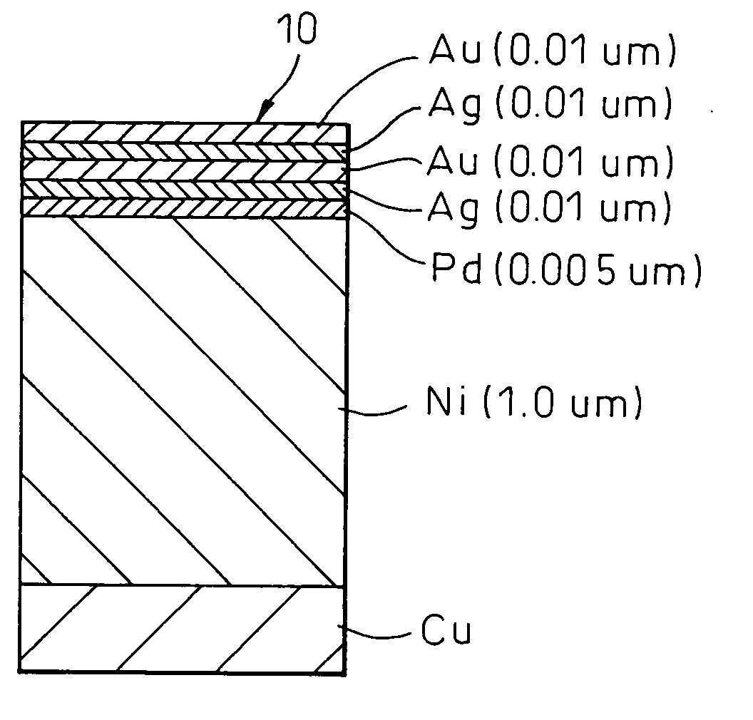
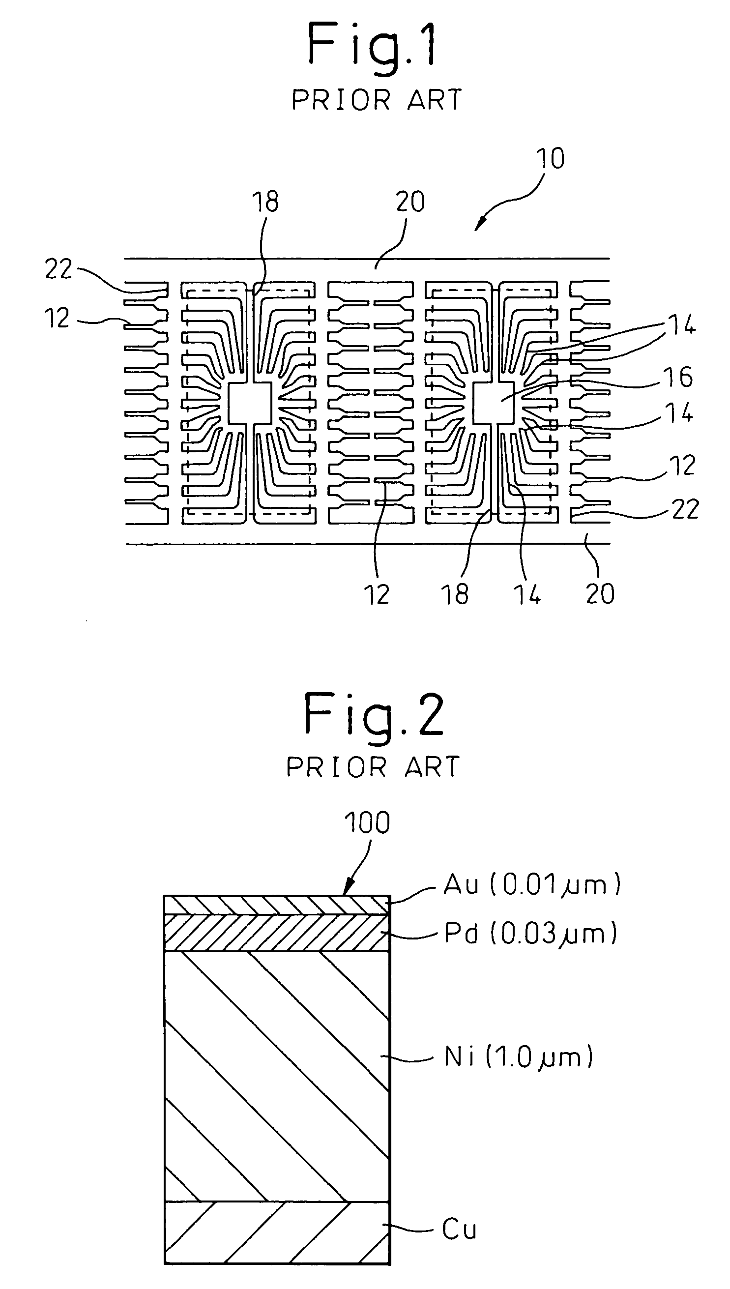
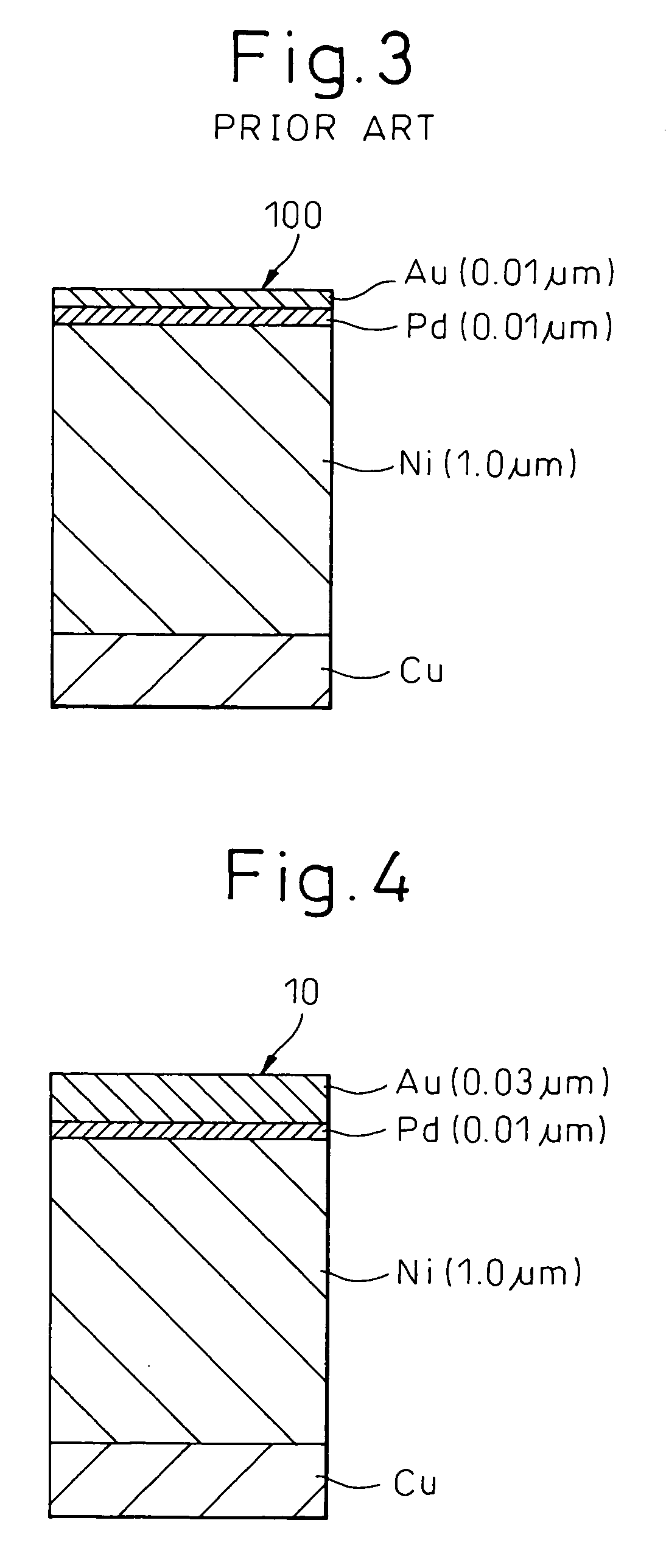
[0028]FIG. 4 is a sectional view illustrating a lead frame according to Example 1 of the present invention. As shown, the lead frame has layers plated on the surface of the substrate of the lead frame to obtain an Au / Pd / Ni lead frame structure. The lead frame 10 for the semiconductor device is produced by forming an Ni-plating layer as an underlayer on the surface of the substrate consisting of Cu, followed by forming a Pd-plating layer on the Ni-plating layer and then forming an Au-plating layer thereon. In this example, the plating conditions such as the plating time and the like are controlled to obtain the Ni-plating layer having a thickness of 1.0 μm, the Pd-plating layer having a thickness of 0.01 μm and the Au-plating layer having a thickness of 0.03 μm. However, it should be noted in this example ...


PUM


Abstract

Lead frames of a Pd-PPF structure for use in a semiconductor device comprising inner leads and outer leads, wherein a whole surface of the substrate constituting the lead frame or at least the outer leads has a composite plated layer, and the composite plated layer comprises an underlayer consisting of an Ni-based plating layer deposited on the whole surface of the substrate constituting the lead frame or on at least the outer leads, a Pd— or Pd alloy-plating layer deposited at a thickness of 0.005 to 0.01 μm on an upper surface of the underlayer, and an Au-plating layer deposited at a thickness of 0.02 to 0.1 μm on an upper surface of the Pd— or Pd alloy-plating layer. When a semiconductor device is mounted on a packaging substrate by using a lead-free Sn—Zn-based solder or any other lead-free solder, the wettability between the lead frame and the lead-free Sn—Zn-based solder or any other lead-free solder is improved to thereby improve the packaging property of the semiconductor device.

Description

TECHNICAL FIELD [0001] The present invention relates to a semiconductor device and, more specifically, to a lead frame for use in a semiconductor device having an improved junction or bonding property and an improved packaging property. BACKGROUND ART [0002] A lead frame for a semiconductor device comprises a stage for mounting a semiconductor chip, inner leads for electric connection to the electrodes of the semiconductor chip through wire bonding, and outer leads used as an external connection terminal when the semiconductor device is mounted on a substrate and the like. Here, it is desired that the stage has a good bonding property to the semiconductor chip, the inner leads have a good wire bonding property, and the outer leads have a good bonding property through soldering to a target member such as a substrate on which the semiconductor device is mounted. [0003]FIG. 1 is a plan view illustrating one example of the lead frame for a semiconductor device. In the lead frame 10, ref...

Claims


Application Information

Patent Timeline
Patent Type & Authority Applications(United States)
IPC IPC(8): H01L23/48H01L23/52H01L23/495H01L23/50
CPCH01L23/49582H01L2224/48247H01L2224/85464H01L2924/01046H01L2924/01078H01L2924/00014H01L2924/01079H01L24/48H01L2224/45099
Inventor SEKI, KAZUMITSUYOSHIE, TAKASHIKADOSAKI, KOICHI
Owner SHINKO ELECTRIC IND CO LTD
Why Eureka
Try Eureka