Method of fabricating polycrystalline silicon

Active Publication Date: 2006-06-15
LG DISPLAY CO LTD
View PDF14 Cites 6 Cited by
  • Summary
  • Abstract
  • Description
  • Claims
  • Application Information

AI Technical Summary

Benefits of technology

[0015] An object of the present invention is to provide a method of fabricating polycrystalline silicon, and a switching device using the fabricated polycr

Problems solved by technology

These non-uniformly crystallized portions cause a reduction in the display quality of an LCD device,

Method used


Image

  • Method of fabricating polycrystalline silicon
  • Method of fabricating polycrystalline silicon
  • Method of fabricating polycrystalline silicon

Examples


Example

[0042] Reference will now be made in detail to the preferred embodiments of the present invention, which are illustrated in the accompanying drawings. Wherever possible, similar reference numbers will be used throughout the drawings to refer to the same or like parts.

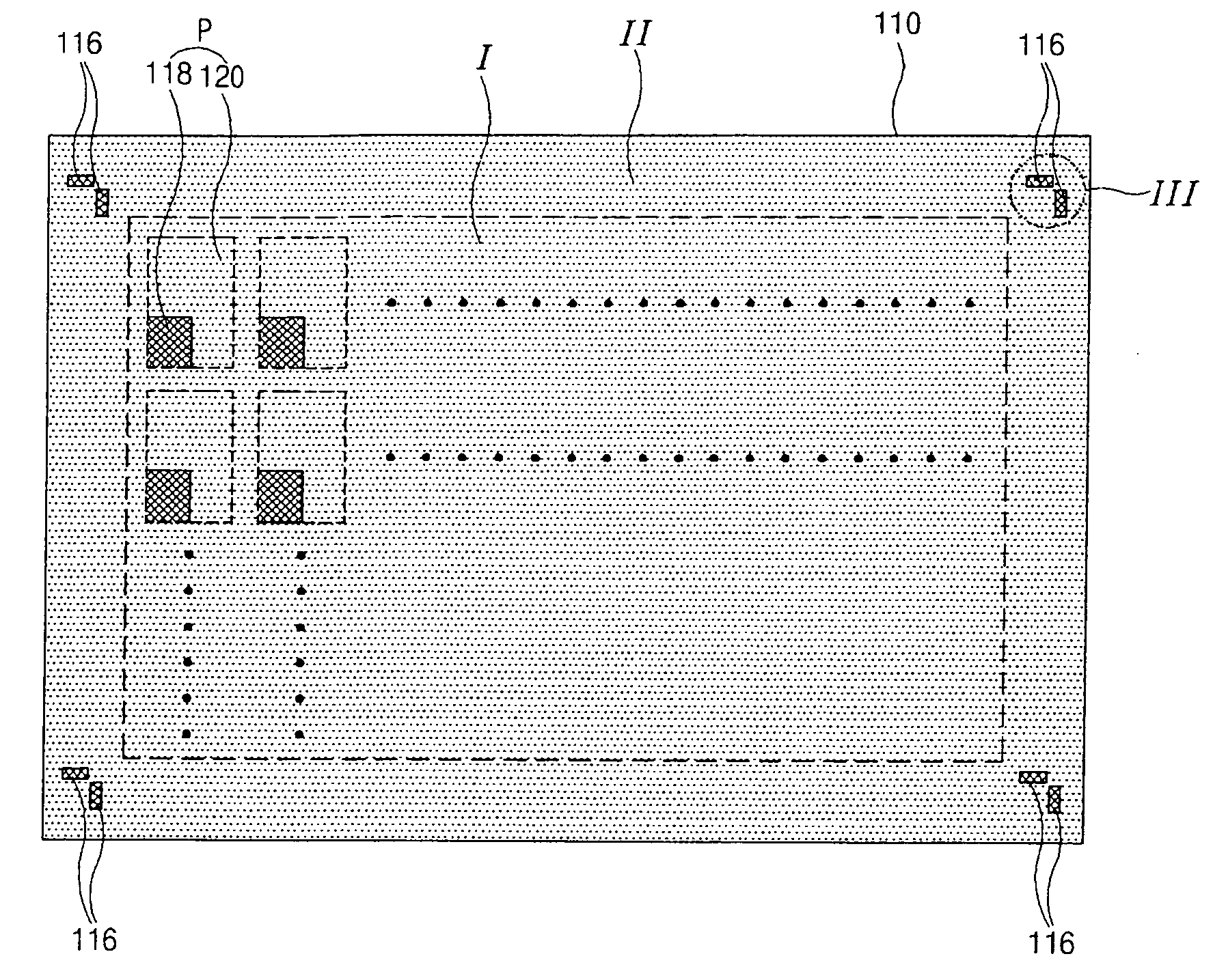
[0043]FIG. 3 is a schematic plane view of a substrate used in a method of fabricating a semiconductor layer of polycrystalline silicon according to the first embodiment of the present invention and FIG. 4 is a magnified plane view of the portion “III” of FIG. 3.

[0044] In FIG. 3, a substrate 110 having a semiconductor layer (114 in FIG. 5) thereon includes a first region “I” and a second region “II” at the periphery of the first region “I.” An align key 116 is formed at each corner portion in the second region “II” of the substrate 110. The first region “I” includes a plurality of pixel regions “P.” The pixel region “P” is a unit region for displaying images, and includes a switching element portion 118 where the semic...


PUM


Abstract

A method of fabricating polycrystalline silicon according to an embodiment includes forming a semiconductor layer of amorphous silicon on a substrate having a first region and a second region surrounding the first region; forming a plurality of flat align keys in the second region using a first mask; forming a plurality of convex align keys by etching the semiconductor layer in the first region, the plurality of convex align keys having steps against the substrate; and crystallizing the semiconductor layer in the first region by aligning a second mask with respect to the plurality of convex align keys.

Description

[0001] The present application is a Divisional of co-pending application Ser. No. 10 / 848,048 filed on May 19, 2004 (now allowed), which is incorporated by reference. The present application also claims the benefit of Korean Patent Application No. 2003-0031810, filed on May 20, 2003 in Korea, which is hereby incorporated by reference for all purposes as if fully set forth herein.BACKGROUND OF THE INVENTION [0002] 1. Field of the Invention [0003] The present invention relates to a method of crystallizing amorphous silicon, and more particularly, to a method of fabricating polycrystalline silicon using an align key and a switching device using the polycrystalline silicon. [0004] 2. Discussion of the Related Art [0005] Flat panel display (FPD) devices having portability and low power consumption have been subject of recent researches in the coming of the information age. Among the various types of FPD devices, liquid crystal display (LCD) devices are widely used as monitors for notebook...

Claims


Application Information

Patent Timeline
IPC IPC(8): H01L23/544G02F1/1368C30B28/10C30B29/06G02F1/13G02F1/136G03F7/00H01L21/00H01L21/027H01L21/20H01L21/268H01L21/306H01L21/324H01L21/336H01L21/77H01L21/84H01L29/786
CPCH01L21/02532H01L21/0268H01L23/544H01L27/1285H01L27/1296H01L29/66757H01L2924/0002H01L2223/5442H01L2223/54453H01L2924/00H01L21/2026H01L29/78675G02F1/136G03F2009/005H01L29/786G03F7/70G02F1/13
Inventor KIM, YOUNG-JOO
Owner LG DISPLAY CO LTD
Why Eureka
Try Eureka