Method for fabricating LCD

Inactive Publication Date: 2007-06-12
LG DISPLAY CO LTD
View PDF255 Cites 4 Cited by
  • Summary
  • Abstract
  • Description
  • Claims
  • Application Information

AI Technical Summary

Benefits of technology

[0029]An advantage of the present invention is to provide a method for fabricating an LCD having the liquid crystal dropping method applied thereto, which can shorten a fabrication time and apply uniform pressure to substrates, to improve productivity.
[0030]Additional features and advantages of the invention will be set forth in the description which follows, and in part will be apparent from the description, or may be learned by practice of the invention. These and other advantages of the invention will be realized and attained by the structure particularly pointed out in the written description and claims hereof as well as the appended drawings.
[0031]To achieve these and other advantages and in accordance with the purpose of the present invention, as embodied and broadly described, a method for fabricating an LCD includes the steps of: (a) loading a first substrate and a second substrate into a bonding chamber; (b) bonding the first and second substrates; (c) venting the bonding chamber to apply pressure to the bonded first and second substrates; and (d) unloading the pressed first and second substrates.
[0032]In one aspect of the present invention, step (a) includes steps of affixing the first and second substrates to lower an

Problems solved by technology

Despite various technical developments in the LCD technology with applications in different fields, research in enhancing the picture quality of the LCD as a display has been in some respects lacking as compared to the features and advantages of the LCD.
However, the related art method for fabricating an LCD having liquid crystal injected therein has the following problems.
First, the related art method has poor productivity because the dipping of the liquid crystal in a liquid crystal bath while the space between the two substrates are maintained at a vacuum and the unit panels are cut into individual pieces for injection of the liquid crystal takes much time.
Second, the liquid crystal injection, for a large LCD in particular, may cause imperfect filling of the liquid crystal in the panel, which may result in a defective panel.
Third, the complicated and lengthy fabrication process requires the use of many liquid crystal injection devices, which occupies a large portion of space.
First, coating the sealant and dropping the liquid crystal on the same substrate requires much fabrication time before the two substrates can be bonded to each other.
Second, as the seal

Method used


Image

  • Method for fabricating LCD
  • Method for fabricating LCD
  • Method for fabricating LCD

Examples


Example

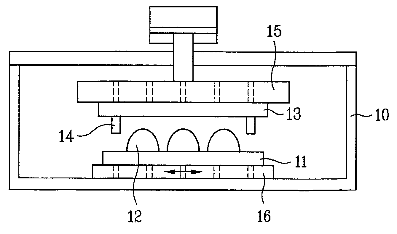
[0046]Reference will now be made in detail to the preferred embodiments of the present invention, examples of which are illustrated in the accompanying drawings.

[0047]FIGS. 2A–2G schematically illustrate the steps of a method for fabricating an LCD in accordance with an embodiment of the present invention.

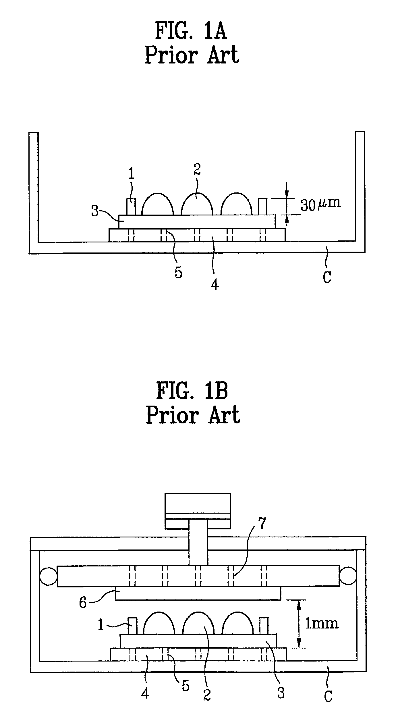
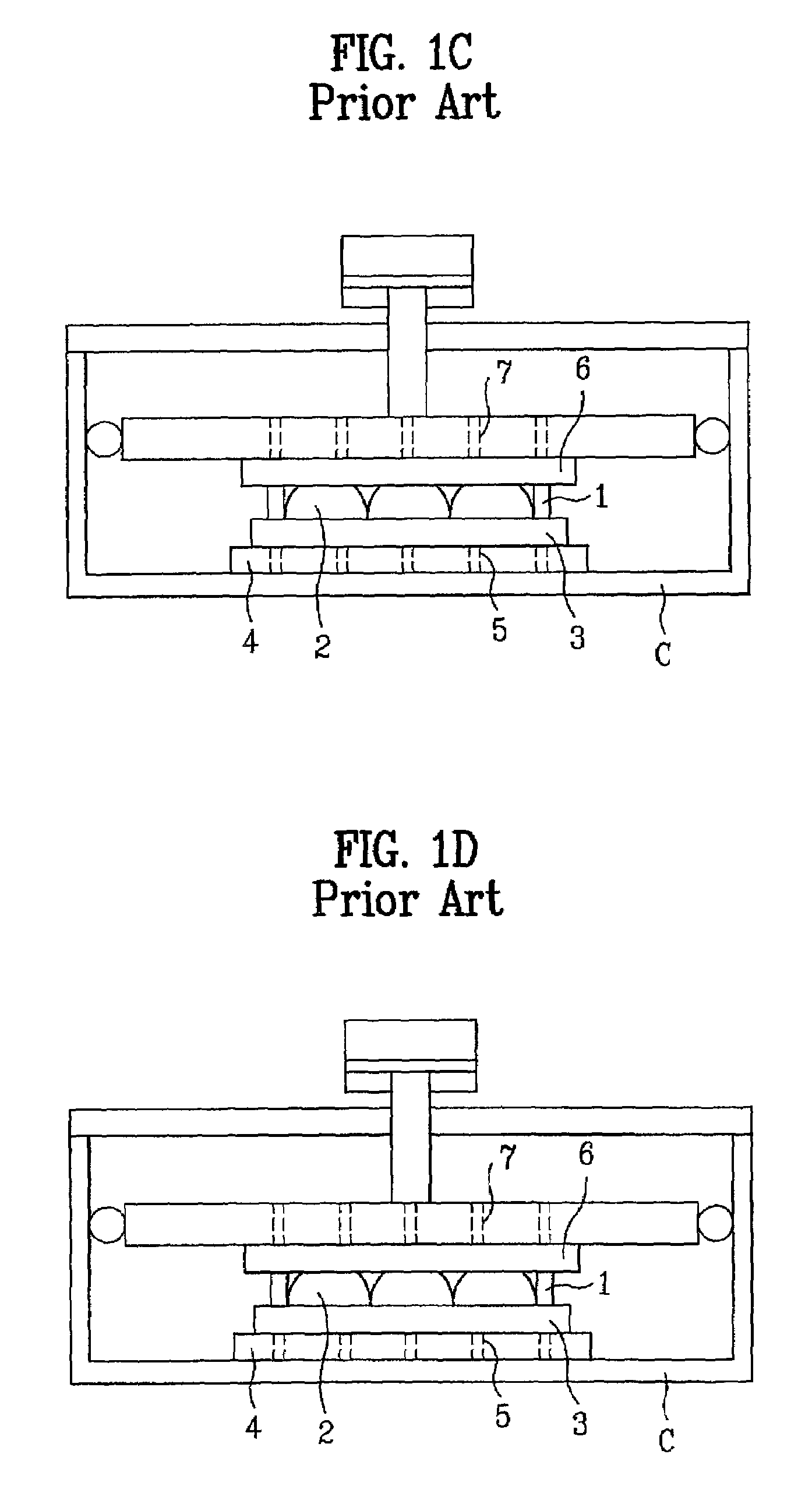
[0048]Referring to FIG. 2A, liquid crystal 12 may be applied to a first glass substrate 11, and seal 14 may be coated on a second substrate 13. A plurality of corresponding areas designated for panels may be provided in first and second glass substrates 11 and 13, and thin film transistor arrays may be formed on each of the panels within the first glass substrate 11 while color filter arrays, black matrix layers, a color filter layers, common electrodes, etc., may be formed on each of the panels of the second glass substrate 13. Liquid crystal material 12 may be applied onto the first glass substrate 11 and a seal 14 may be coated onto the second glass substrate 13. Alternatively, ...


PUM


Abstract

A method for fabricating an LCD by liquid crystal dropping includes the steps of (a) loading a first substrate and a second substrate on a bonding chamber, (b) bonding the first and second substrates, (c) venting the bonding chamber for applying a pressure to the bonded first and second substrates, and (d) unloading the pressed first and second substrates.

Description

[0001]This application claims the benefit of the Korean Application Nos. P2002-8319 filed on Feb. 16, 2002, and P2002-8424 filed on Feb. 18, 2002, which are hereby incorporated by reference.[0002]This application incorporates by reference two co-pending applications, Ser. No. 10 / 184,096, filed on Jun. 28, 2002, entitled “SYSTEM AND METHOD FOR MANUFACTURING LIQUID CRYSTAL DISPLAY DEVICES” and Ser. No. 10 / 184,088, filed on Jun. 28, 2002, entitled “SYSTEM FOR FABRICATING LIQUID CRYSTAL DISPLAY AND METHOD OF FABRICATING LIQUID CRYSTAL DISPLAY USING THE SAME”, as if fully set forth herein.BACKGROUND OF THE INVENTION[0003]1. Field of the Invention[0004]The present invention relates to a liquid crystal display, and more particularly, to a method for fabricating an LCD having a liquid crystal dropping method applied thereto.[0005]2. Discussion of the Related Art[0006]In general, recent developments in the information communication field have increased demand for various types of display dev...

Claims


Application Information

Patent Timeline
IPC IPC(8): G02F1/13G02F1/1341
CPCG02F1/1341G02F2001/13415G02F1/13415
Inventor LEE, SANG SEOKPARK, SANG HOLEE, LIM SU
Owner LG DISPLAY CO LTD
Why Eureka
Try Eureka