Organic EL devices

Inactive Publication Date: 2006-06-15
TOYOTA IND CORP
View PDF3 Cites 40 Cited by
  • Summary
  • Abstract
  • Description
  • Claims
  • Application Information

AI Technical Summary

Benefits of technology

[0009] As noted above, no organic EL device has been obtained yet which simultaneously has good whiteness, light-emitting efficiency, and lifetime. Considering th

Problems solved by technology

As noted above, no organic EL device has been obtained yet which simul

Method used


Image

  • Organic EL devices
  • Organic EL devices
  • Organic EL devices

Examples


Example

Example 1

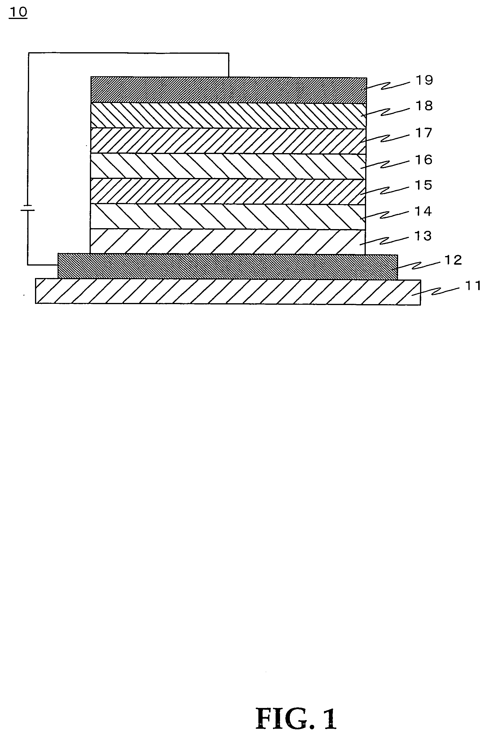
[0123] A transparent glass substrate (11), on one of whose surfaces an anode (12) made of an ITO layer of 150 nm thickness had been formed, was washed with an alkali and then with pure water, dried, and then cleaned with UV-ozone.

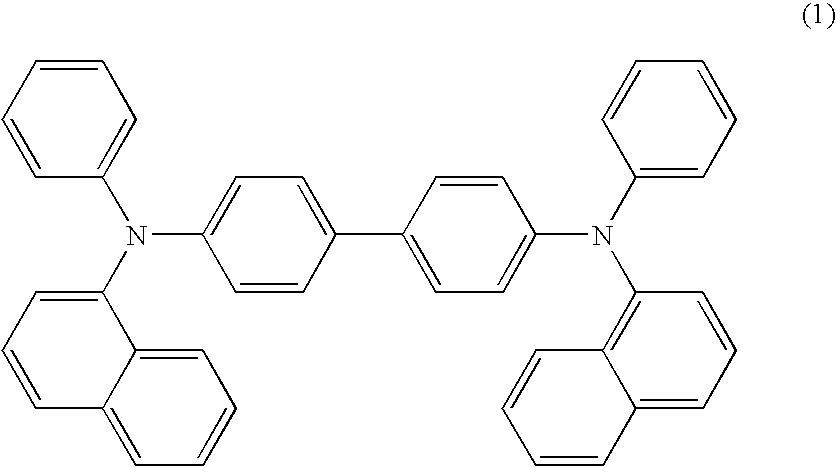
[0124] Onto the anode (12) on the thus washed substrate (11), NPB of the following formula (1) was vapor-deposited in a vacuum vapor deposition apparatus (a carbon crucible, at a vapor deposition speed of 0.1 nm / s, in vacuo around 5.0×10⁻⁵ Pa) to prepare a 40 nm thickness layer to be a hole-transporting layer (13).

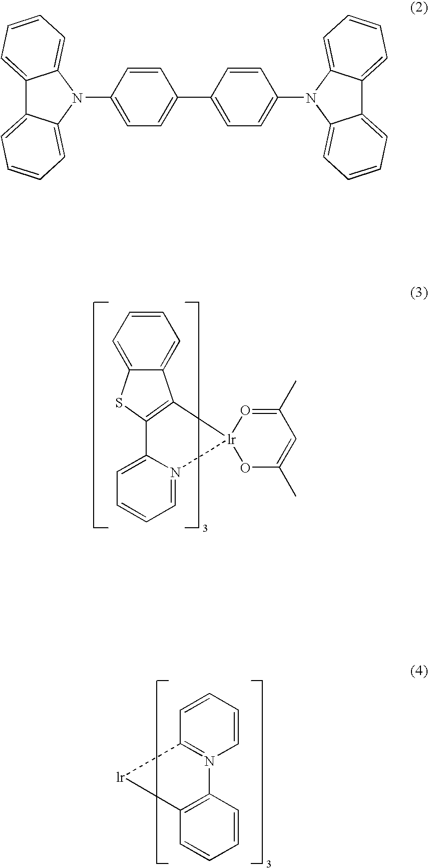
[0125] Onto the hole-transporting layer (13), 89.5 weight % of a phosphorescent host CBP of the following formula (2), 0.5 weight % of a red phosphorescent dopant btP2Ir(acac) of the following formula (3), and 10 weight % of a green phosphorescent dopant Ir(ppy)3 of the following formula (4) were co-vapor-deposited in a vacuum vapor deposition apparatus (a carbon crucible, at a vapor deposition speed of 0.1 nm / s, in vacuo around 5.0×1...

Example

Example 2

[0134] In example 2, the phosphorescent light-emitting layer (14) as in example 1 was divided into a red phosphorescent light-emitting layer of 1 nm thickness comprising 5 weight % of a red phosphorescent dopant and a green phosphorescent light-emitting layer of 8 nm thickness comprising 10 weight % of a green phosphorescent dopant. As the hosts of both the phosphorescent light-emitting layers, the red phosphorescent dopant, and the green phosphorescent dopant, the same materials as in example 1 were used. Except for the lamination order of the phosphorescent and fluorescent light-emitting layers being altered as shown in TABLE 1, an organic EL device was prepared similar to example 1. In example 2, the thickness of the red phosphorescent light-emitting layer was 1 nm, which was thinner than that of a single-molecular film of the phosphorescent host CBP, so the red phosphorescent light-emitting layer was an island thin film. Similarly to example 1, the electric power effic...

Example

Example 3

[0135] In example 3, an organic EL device was prepared similarly to in example 1 except that the non-light-emitting interface layer was made only of a hole-transporting material CuPc. Similar to example 1, the electric power efficiency, etc. of the prepared organic EL device were measured. The results obtained are shown in TABLE 2 wherein the electric power efficiency and the half-life are shown as relative values with respect to those of example 1. TABLE 2electricchroma-chroma-interface layerpowerticityticityexamples(weight %)efficiencyxyhalf-life1NPB:BCP10.320.331(50:50)3CuPc0.940.300.300.92(100)


PUM

PropertyMeasurementUnit
Percent by massaaaaaaaaaa
Thicknessaaaaaaaaaa

Abstract

Organic EL devices having a light-emitting layer comprising a fluorescent dopant, a light-emitting layer comprising a phosphorescent dopant, and a non-light-emitting interface layer provided between an anode and a cathode wherein the light-emitting layer comprising a fluorescent dopant is provided nearer to the cathode than the light-emitting layer comprising a phosphorescent dopant and wherein the non-light-emitting interface layer is provided between the light-emitting layer comprising a fluorescent dopant and the light-emitting layer comprising a phosphorescent dopant.

Description

FIELD OF THE INVENTION [0001] The present invention relates to organic electroluminescence (EL) devices. BACKGROUND OF THE INVENTION [0002] Recently, there are great expectations towards applications of organic EL devices in full-color display devices. As one method for full-color displays using an organic EL device, a method is known where white light emitted by the device is divided into red, green, and blue lights by color filters and the following properties are required in organic EL devices used for such purposes: i) Good balance amongst the light-emitting intensities of red, green, and blue and a resulting good whiteness; ii) High light-emitting efficiency; iii) Long lifetime. [0003] As an organic EL device whose above properties are relatively good one has been proposed wherein a blue fluorescent dopant, a red phosphorescent dopant, and a green phosphorescent dopant are contained in the same light-emitting layer, for example, as seen in JP2004-14155A. [0004] In such organ...

Claims


Application Information

Patent Timeline
IPC IPC(8): H01L51/50
CPCH01L51/005H01L51/0052H01L51/0059H01L51/0062H01L51/0081H01L51/0085H01L51/5016H01L51/504H01L51/5044H01L2251/5376H10K85/60H10K85/649H10K85/615H10K85/631H10K85/324H10K85/342H10K50/131H10K50/13H10K50/11H10K2101/10H10K2101/27H05B33/14H05B33/18
Inventor NAGARA, YOSHIAKIIIJIMA, TOSHIKIKAWASUMI, KAZUHITO
Owner TOYOTA IND CORP
Why Eureka
Try Eureka