Solid-state image pickup element and image pickup apparatus using the same

a technology of image pickup and image, which is applied in the direction of television system, television system scanning details, radioation control devices, etc., can solve the problems of impaired performance of photoelectric conversion elements which have been previously formed, and obvious performance impairment of photoelectric converting elements, so as to increase the amount of signal charges and increase the capacity of signal charge transfer of vertical transfer paths

Inactive Publication Date: 2006-06-15
FUJIFILM HLDG CORP +1
View PDF5 Cites 12 Cited by
  • Summary
  • Abstract
  • Description
  • Claims
  • Application Information

AI Technical Summary

Benefits of technology

[0011] According to the configuration, the signal charge transfer capacity of the vertical transfer paths can be increased, and hence it is possib

Problems solved by technology

On the other hand, the photoelectric converting films stacked above the semiconductor substrate are made of organic materials, and hence their performance is obviously impaired when exposed to a high temperature of 200 degrees or higher.
In the stack-type solid-state image pickup element, for example, a production step

Method used


Image

  • Solid-state image pickup element and image pickup apparatus using the same
  • Solid-state image pickup element and image pickup apparatus using the same
  • Solid-state image pickup element and image pickup apparatus using the same

Examples


first embodiment

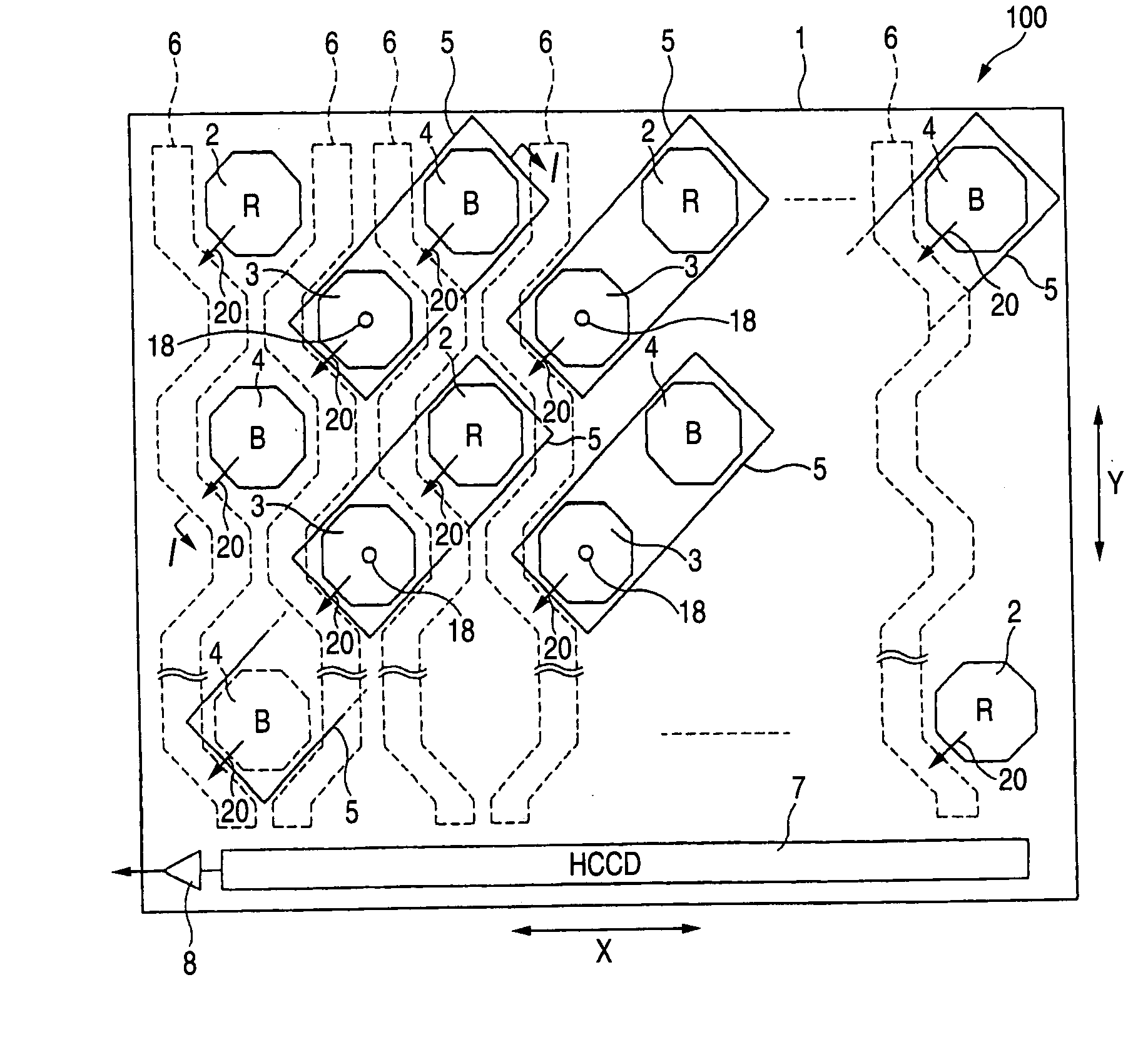
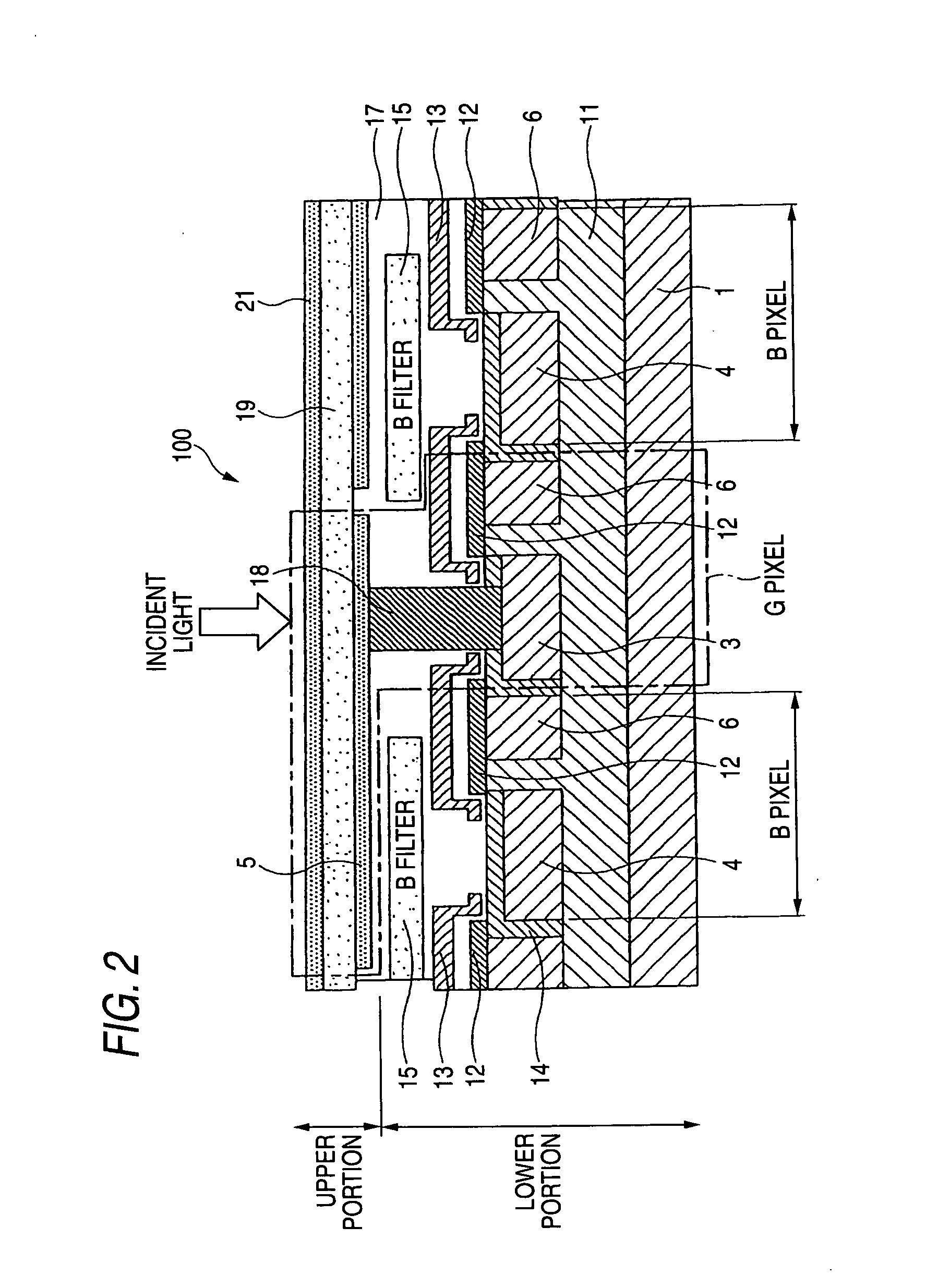
[0038]FIG. 1 is a surface diagram of a solid-state image pickup element 100 illustrating a first embodiment of the invention, and FIG. 2 is a cross-sectional diagram taken along the line I-I of FIG. 1.

[0039] On a surface portion of a semiconductor substrate 1, plural photoelectric converting elements 2, 4 made of silicon, and plural signal charge accumulating portions 3 are arranged in the row direction (the X direction in FIG. 1) and the column direction (the Y direction in FIG. 1). In the embodiment, it is assumed that the total number of the photoelectric converting elements 2 and the photoelectric converting elements 4 is equal to the number of the signal charge accumulating portions 3. The number of the signal charge accumulating portions 3 is equal to the maximum pixel data number of color image data which can be produced on the basis of color signals obtained from the solid-state image pickup element 100.

[0040] As shown in FIG. 1, in the odd rows, the photoelectric converti...

second embodiment

[0066] In the solid-state image pickup element 100, as shown in FIG. 2, the aperture ratio of the R photoelectric converting elements 2 and the B photoelectric converting elements 4 which are disposed in the lower portion is very smaller than that of the photoelectric converting film 19 which is disposed in the upper portion. When a fixed amount of light is incident on the solid-state image pickup element 100, the amount of light incident on the R photoelectric converting elements 2 and the B photoelectric converting elements 4 which are disposed in the lower portion is smaller than that of light incident on the photoelectric converting film 19 because of influences due to the color filters, the light shielding film 13, the vertical conductors 18, the aperture ratio, etc. Therefore, the sensitivities of color signals obtained from the upper portion and the lower portion may be dispersed, or the S / N (Signal to Noise ratio) of a color signal obtained from the lower portion may be impa...

third embodiment

[0108] In a solid-state image pickup element in which, as shown in FIG. 1, green signals the number of which is equal to that of all pixel data of color image data are output, and red and blue signals the numbers of which are smaller than the number of all pixel data of color image data are output, a process of interpolating the red and blue signals is performed, and hence there is the possibility that a false color is generated. In the embodiment, a signal process in which generation of such a false color can be suppressed will be described. The signal process is implemented in the digital signal processing section 36 or the analog signal processing section 32 shown in FIG. 6.

[0109] Hereinafter, a signal processing method will be described with using: color signals obtained from nine or 3-row by 3-column photoelectric converting elements centered at the photoelectric converting element 2 or 4 corresponding to one pixel data of color image data; and color signals obtained from nine...


PUM


Abstract

A solid-state image pickup element has: a photoelectric converting film which is stacked above a semiconductor substrate; plural photoelectric converting elements which are arranged in the row direction and the column direction on the semiconductor substrate, and signal charge accumulating portions in which signal charges generated in the photoelectric converting film are accumulated; vertical transfer paths which are formed in the semiconductor substrate, and which transfer signal charges accumulated in the photoelectric converting elements and the signal charge accumulating portions, in the column direction; a horizontal transfer path which transfers the signal charges transferred from the vertical transfer paths, in the row direction; and an output section which outputs color signals corresponding to the signal charges transferred from the horizontal transfer path. The vertical transfer paths are formed so that two of them are disposed between the photoelectric converting elements adjacent to each other in the row direction, and between the signal charge accumulating portions, and they are formed so as to meander in the column direction between the columns.

Description

BACKGROUND OF THE INVENTION [0001] 1. Field of the Invention [0002] The present invention relates to a solid-state image pickup element in which signal charges are transferred by CCDs and an image pickup apparatus using the same. [0003] 2. Description of the Related Art [0004] In the related art, as a solid-state image pickup element in which a color filter is not used, a stack-type solid-state image pickup element disclosed in, for example, JP-A-2002-83946 has been proposed. The stack-type solid-state image pickup element has a configuration where photoelectric converting films made of three organic materials which respectively detect red (R) light, green (G) light, and blue (B) light are stacked above a semiconductor substrate, signal charges generated in the films are accumulated in accumulation diodes formed on the semiconductor substrate, and the signal charges accumulated in the accumulation diodes are read out by a signal read circuit such as vertical CCDs and a horizontal CC...

Claims


Application Information

Patent Timeline
IPC IPC(8): H04N5/335H01L27/146H01L27/148H04N5/357H04N5/369H04N5/372H04N5/3728H04N9/07
CPCH01L27/14621H01L27/14645
Inventor INUIYA, MASAFUMI
Owner FUJIFILM HLDG CORP
Why Eureka
Try Eureka