Solid-state imaging device having a punch-through stopper region positioned closer to a signal accumulation region than is an end of the drain region

a solid-state imaging and punch-through stopper technology, which is applied in the direction of diodes, semiconductor devices, radio frequency controlled devices, etc., can solve the problems of inability to solve the problem, the signal charge of the photodiode 211 cannot be completely transferred, and the channel modulation by the gate voltage becomes less effective, etc., to increase the amount of signal charge accumulation, increase the effect of signal charge accumulation

Active Publication Date: 2008-01-08
COLLABO INNOVATIONS INC
View PDF2 Cites 4 Cited by
  • Summary
  • Abstract
  • Description
  • Claims
  • Application Information

AI Technical Summary

Benefits of technology

[0020]Considering the aforementioned problems, an object of the present invention is to provide a solid-state imaging device which can increase the amount of signal charge accumulation in the photodiode, and a manufacturing method thereof.
[0030]Therefore, the present invention can provide a solid-state imaging device which can increase the amount of signal charge accumulation in the photodiode and a manufacturing method thereof. The practical value of the present invention is thus very high.

Problems solved by technology

However, when the semiconductor substrate 221 has a high impurity concentration, the channel modulation by the gate voltage becomes less effective and the signal charge of the photodiode 211 cannot be transferred completely.
Accordingly, this method cannot solve the problem.

Method used


Image

  • Solid-state imaging device having a punch-through stopper region positioned closer to a signal accumulation region than is an end of the drain region
  • Solid-state imaging device having a punch-through stopper region positioned closer to a signal accumulation region than is an end of the drain region
  • Solid-state imaging device having a punch-through stopper region positioned closer to a signal accumulation region than is an end of the drain region

Examples


Embodiment Construction

[0049]Hereafter, a solid-state imaging device according to an embodiment of the present invention is described with reference to the drawings.

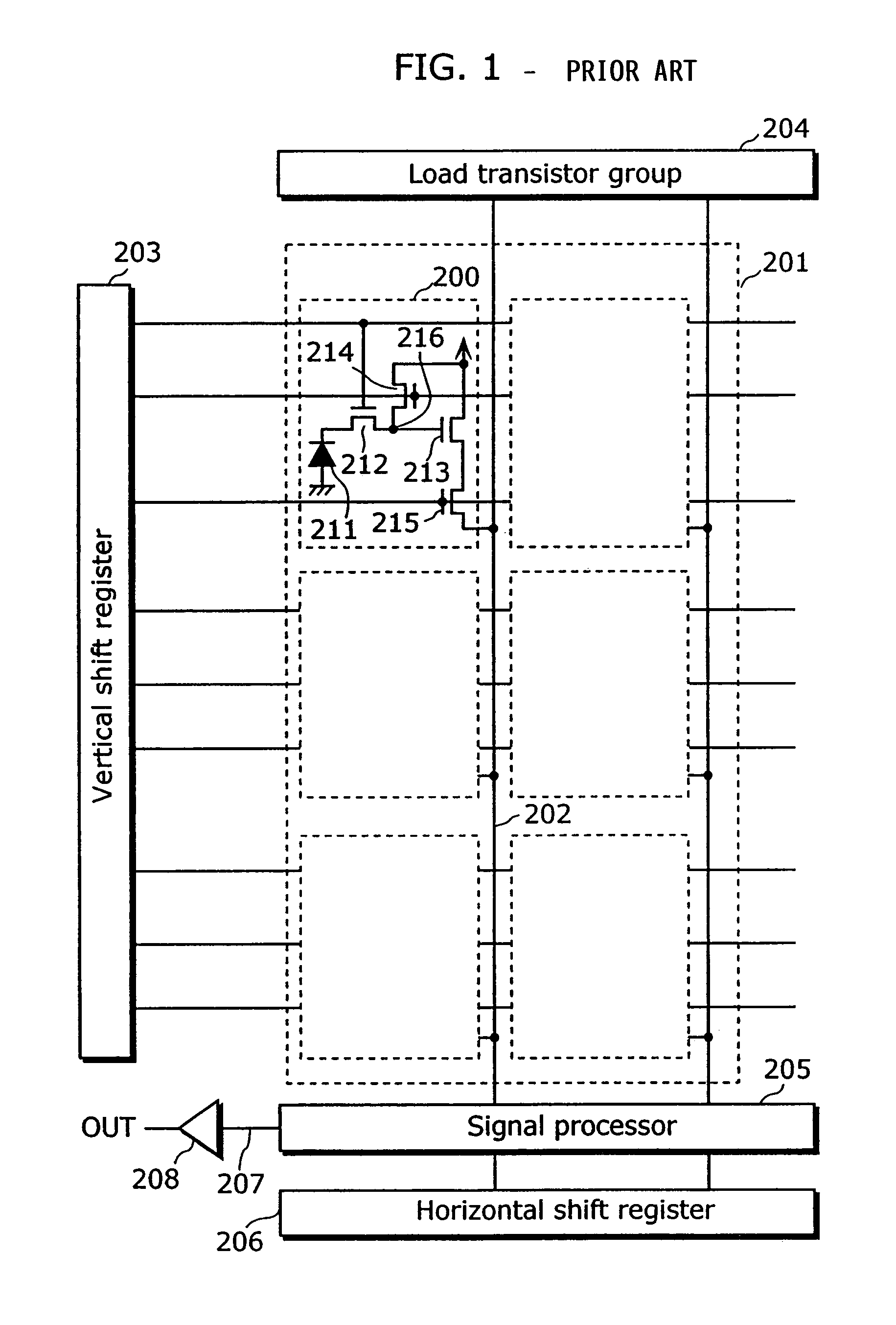
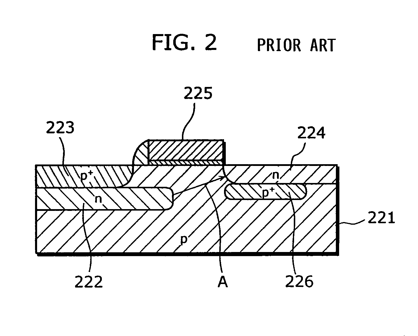
[0050]FIG. 5 is a circuit diagram showing a structure of a MOS-type solid-state imaging device according to the present embodiment. In FIG. 5, the same reference numbers are assigned to the same constituents as shown in FIG. 1, and detailed explanations about them are omitted here.

[0051]The MOS-type solid-state imaging device according to the present embodiment is made up of an image area 101 in which n×m unit cells 100 are two-dimensionally arranged, a first vertical signal line 202, a vertical shift register 203, a load transistor group 204, a signal processor 205, a horizontal shift register 206, a horizontal signal line 207, and an output amplifier 208.

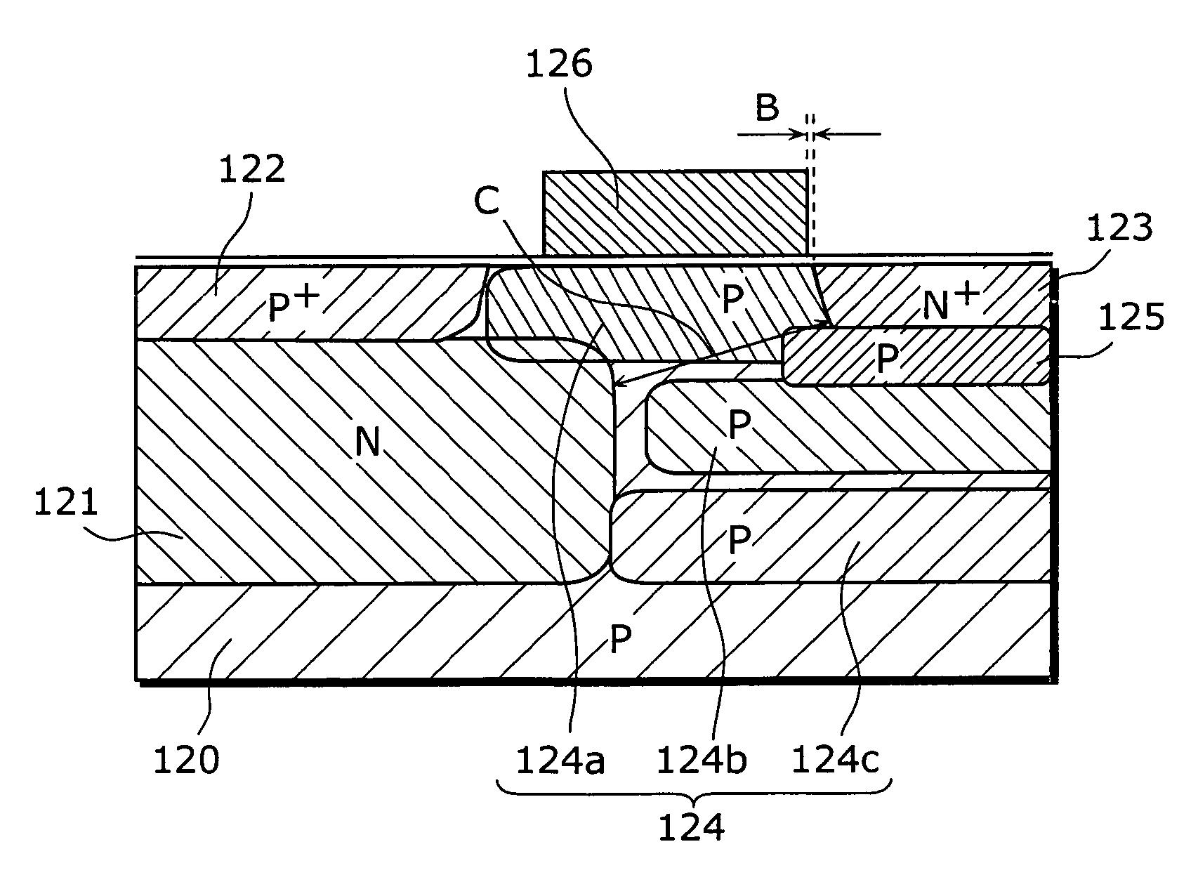
[0052]Each of the unit cells 100 includes a photodiode 111 which converts an optical signal into signal charge, a read-out transistor 112 which reads out the signal of the photodiode 111, an...


PUM


Abstract

A solid-state imaging device can increase the amount of signal charge accumulation in a photodiode. The solid-state imaging device includes a gate electrode formed on a p-type semiconductor substrate. An n-type signal accumulation region accumulates the signal charge obtained through a photo-electrical conversion, and is formed in the semiconductor substrate so that a portion of the signal accumulation region is positioned below the gate electrode. An n-type drain region is positioned in the semiconductor substrate so that the n-type drain region is positioned opposite the signal accumulation region across the gate electrode. A p-type punch-through stopper region has a higher impurity concentration than the semiconductor substrate, and is formed in the semiconductor substrate so that the p-type punch-through region is positioned below the drain region, wherein an end of the punch-through stopper region is positioned closer to the signal accumulation region than the end of the drain region.

Description

BACKGROUND OF THE INVENTION[0001](1) Field of the Invention[0002]The present invention relates to a solid-state imaging device, and in particular to a solid-state imaging device having an improved read-out transistor portion which reads out signal charge from a photodiode, and to a manufacturing method thereof.[0003](2) Description of the Related Art[0004]Conventionally, solid-state imaging devices such as a Charge-Coupled Device (CCD) solid-state imaging device and a metal-oxide semiconductor (MOS) solid-state imaging device are used for various image input apparatuses such as video cameras, digital still cameras and facsimiles. The solid-state imaging devices are mainly used for portable apparatuses and low-voltage drive is required for the solid-state imaging devices. A solid-state imaging device responding to this requirement is disclosed, for example, in Japanese Laid-Open Patent Application No. 2000-150847.[0005]FIG. 1 is a circuit diagram showing a structure of a conventional...

Claims


Application Information

Patent Timeline
Patent Type & Authority Patents(United States)
IPC IPC(8): H01L31/062H01L27/146
CPCH01L27/14632H01L27/14643H01L27/14687H01L27/14689H01L31/035236H01L27/146
Inventor TANAKA, SYOUJIMIYAGAWA, RYOHEIKOGA, KAZUNARIHIRATA, TATSUYANAGASAKI, HIROKI
Owner COLLABO INNOVATIONS INC
Why Eureka
Try Eureka