Differential amplifier

a technology of amplifiers and amplifiers, applied in the field ofdifferential amplifiers, can solve the problems of deteriorating system characteristics, inability to obtain desired characteristics, and inability to successfully process input signals, etc., to achieve the effect of increasing the signal amount, reducing the amount of signals, and increasing the minimum value of signals outpu

Active Publication Date: 2011-03-01
RENESAS ELECTRONICS CORP
View PDF5 Cites 4 Cited by
  • Summary
  • Abstract
  • Description
  • Claims
  • Application Information

AI Technical Summary

Benefits of technology

[0020]According to the present invention, when the first MOS transistor operates to increase the amount of the signal flowing through the source and the drain thereof, the second MOS transistor operates to decrease the amount of the signal. This produces an effect of increasing a minimum value of the signal output by the differential amplifier. This is because the second MOS transistor has a function of confining the maximum current originally caused to flow by the first MOS transistor. Further, when the first MOS transistor operates to increase the amount of the signal flowing between the source and the drain thereof, the third MOS transistor operates to increase the amount of the signal. This ensures a small signal gain comparable to or better than the conventional differential amplifier in the high frequency region. Therefore, the minimum value of the output signal is increased while maintaining the small signal gain in the high frequency region, to thereby realize the limiter operation even in the high frequency region.
[0021]The present invention enables the differential amplifier to perform the limiter operation also on the signal having the high frequency, and hence to perform the limiter operation even when the differential amplifier amplifies a signal having a wide frequency range, that is, a wide band signal. Further, according to the present invention, the following two effects may be obtained: the differential amplifier may have a good frequency characteristic in a wide band; and the gain of the differential amplifier is enhanced.

Problems solved by technology

This is because when a signal having a large amplitude above the certain range or a signal having an amplitude that is within the certain range but too small is input to the demodulation circuit 1008, desired characteristics are not obtained, resulting in deteriorated characteristics due to the system design.
This waveform distortion makes it impossible to obtain the desired characteristics.
On the other hand, for example, in the case of the signal having the small amplitude as described above, the waveform input to the demodulation circuit 1008 is buried in noise due to a low signal to noise (S / N) ratio and the demodulation circuit 1008 may not be able to successfully process the input signal.
This is disadvantageous in limiting the amplitude of the signal input to the demodulation circuit 1008 to the certain range, and hence it is necessary to uniquely determine the gain of the mixer 1005.
In such a case, it becomes difficult for the differential amplifier using the resistors as the loads Z1 and Z2 to perform the limiter operation on the signal having such high frequency.
Then, the value of each of the signals output from the differential amplifier does not take the constant maximum value and minimum value for performing the limiter operation, and it becomes difficult to perform the limiter operation.
Under such a situation, it is impossible to obtain the desired high gain and the limiter operation, and hence it becomes impossible to set the gain of the mixer 1005 constant.
However, when the inductors are used as the loads Z1 and Z2 of the differential amplifier, it becomes difficult to make the differential amplifier perform the limiter operation.
However, it is required for the differential amplifier to amplify the input signal with a correspondingly higher amplification factor, and it becomes difficult to perform the limiter operation.
As described above, according to the conventional technology, the attempt to make the amplitude of each of the signals output by the differential amplifier constant fails to appropriately make the amplitude constant for the input signal having the high frequency because a gain drop occurs, and the attempt to increase the decreasing gain makes it difficult to realize the limiter operation of the differential amplifier that makes the amplitude constant.
Consequently, the conventional technology has had a technical problem to be solved in that it is difficult for the differential amplifier that amplifies the signal having the high frequency to make the amplitude of each output signal constant.

Method used


Image

  • Differential amplifier
  • Differential amplifier
  • Differential amplifier

Examples


first embodiment

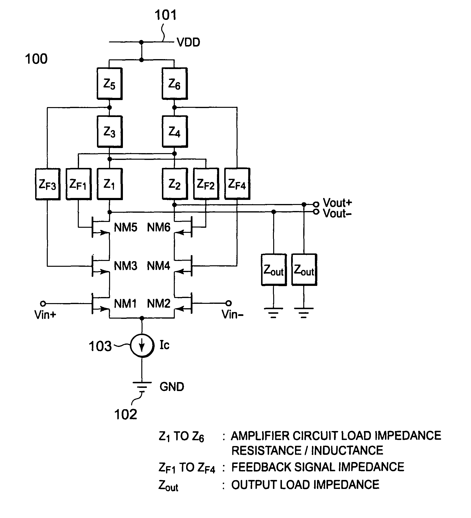
[0040]FIG. 1 illustrates a differential amplifier 100 according to a first embodiment of the present invention. First, a configuration of the differential amplifier 100 is described. Circuit elements constituting the differential amplifier 100 are provided between a power supply line 101, which supplies a power supply voltage VDD, and a ground line 102, which defines a reference potential. A constant current source 103 is a current source that supplies a current of a constant current value Ic. Transistors NM1, NM2, NM3, NM4, NM5, and NM6 are n-type MOS transistors, and each has a gate for controlling a channel formed between a source and a drain to be ON and OFF. The source of the MOS transistor NM1 and the source of the MOS transistor NM2 are connected to the constant current source 103. The gate of the MOS transistor NM1 is connected to an input terminal Vin+. A first input signal to be amplified is input to the input terminal Vin+. On the other hand, the gate of the MOS transisto...

second embodiment

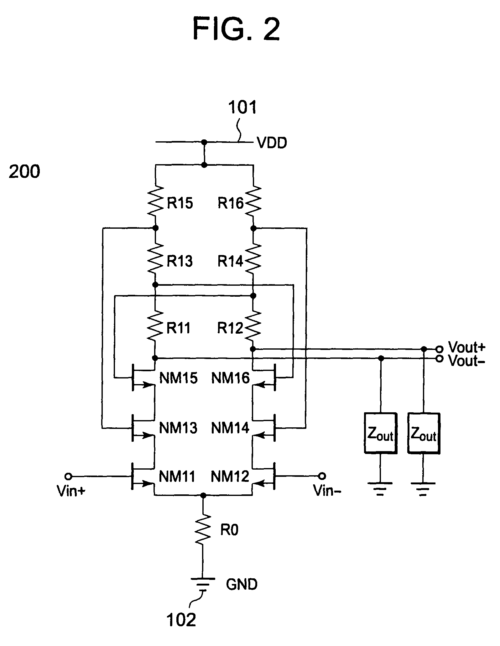
[0062]FIG. 5 illustrates a differential amplifier 500 according to a second embodiment of the present invention. The differential amplifier 500 according to the second embodiment is different from the differential amplifier 200 according to the first embodiment in that each of the first load circuit and the second load circuit includes inductors as well as a resistor. Specifically, the loads Z1 and Z3 in the first load circuit are the inductors, and the loads Z2 and Z4 in the second load circuit are the inductors.

[0063]By using the inductors in the first load circuit and the second load circuit, the differential amplifier 500 may achieve a high gain in a higher frequency region than the differential amplifier 200 according to the first embodiment. NMOS transistors NM23 and NM24 operate in a linear region as in the first embodiment, and have a function of suppressing a current caused to flow by NMOS transistors NM21 and NM22 and hence increasing a lower limit of a limiter operation d...

third embodiment

[0066]FIG. 8 illustrates a differential amplifier 800 according to a third embodiment of the present invention. The differential amplifier 800 according to the third embodiment is different from each of the differential amplifiers according to the first and second embodiments in that inductors and p-type MOS transistors are used in combination as the loads, and a wide frequency band may be covered by switching a load inductance used in an operation of the differential amplifier. In this case, a combination of a PMOS transistor PM37 and an inductor L31 or a combination of an inductor L33 and a PMOS transistor PM39 is the first load circuit. Similarly, a combination of an inductor L32 and a PMOS transistor PM38 or a combination of an inductor L34 and a PMOS transistor PM40 may be the second load circuit. Each of the inductors L31 and L32 is the load inductance to support a high frequency band. On the other hand, each of the inductors L33 and L34 is the load inductance to support a low...


PUM


Abstract

In a wireless communications system, it is important to realize a limiter operation by which a differential amplifier for amplifying a local signal may stably supply an output signal having a constant amplitude. However, when a signal handled by the system has a high frequency, a gain of the differential amplifier is reduced and the limiter operation may not be performed appropriately. The differential amplifier is configured employing a double cascode connection to enhance an output impedance, an upper transistor of the double cascode connection realizes enhancement in gain and frequency characteristics based on a positive feedback signal, and a lower transistor of the double cascode connection controls an operating point and suppresses an allowable output voltage range by operating in a linear region and based on a negative feedback signal to facilitate the limiter operation.

Description

BACKGROUND OF THE INVENTION[0001]1. Field of the Invention[0002]The present invention relates to a differential amplifier, and more particularly, to a differential amplifier that performs a limiter operation and needs to operate at a high frequency and in a wide band.[0003]2. Description of the Related Art[0004]In recent years, through an improvement in microprocessing technology for manufacturing semiconductor devices, a complementary metal-oxide semiconductor (CMOS) transistor has found its use in a radio frequency (RF) circuit using a gigahertz frequency band, thereby becoming available to form the RF circuit for handling a high frequency band signal and a circuit for handling a baseband signal on one chip.[0005]FIG. 10 illustrates a configuration of a transceiver system of a terminal for wireless communications using frequency bands of several gigahertz. Note that in FIG. 10, each of a transmitter circuit and a receiver circuit has one signal line. However, any one of the transm...

Claims


Application Information

Patent Timeline
Patent Type & Authority Patents(United States)
IPC IPC(8): H03F3/45
CPCH03F3/195H03F3/45188H03F2200/451H03F2203/45318H03F2203/45352H03F2203/45516H03F2203/45528H03F2203/45638H03F2203/45641H03F2203/45644H03F2203/45648H03F2203/45698H03F2203/45702
Inventor MATSUI, NAOHIRO
Owner RENESAS ELECTRONICS CORP
Why Eureka
Try Eureka