Solid-state imaging device and manufacturing method thereof
- Summary
- Abstract
- Description
- Claims
- Application Information
AI Technical Summary
Benefits of technology
Problems solved by technology
Method used
Image
Examples
Embodiment Construction
[0049] Hereafter, a solid-state imaging device according to an embodiment of the present invention is described with references to the drawings.
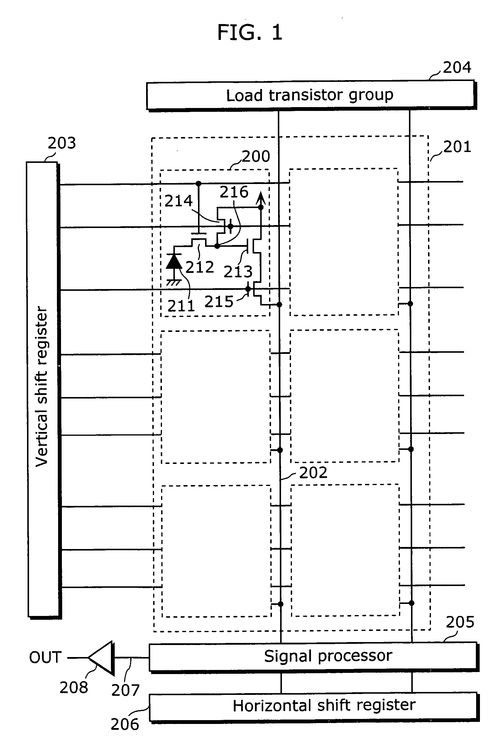
[0050]FIG. 5 is a circuit diagram showing a structure of a MOS-type solid-state imaging device according to the present embodiment. In FIG. 5, same reference numbers are assigned to the same constituents as shown in FIG. 1, and detailed explanations about them are omitted here.
[0051] The MOS-type solid-state imaging device according to the present embodiment is made up of an image area 101 in which n×m unit cells 100 are two-dimensionally arranged, a first vertical signal line 202, a vertical shift register 203, a load transistor group 204, a signal processor 205, a horizontal shift register 206, a horizontal signal line 207, and an output amplifier 208.
[0052] Each of the unit cells 100 includes a photodiode 111 which converts an optical signal into signal charge, a read-out transistor 112 which reads out the signal of the photodiode 111,...
PUM
 Abstract
Description
Claims
Application Information


