Ruthenium as an underlayer for tungsten film deposition

a technology of tungsten film and ruthenium, which is applied in the direction of chemical vapor deposition coating, transportation and packaging, coating, etc., can solve the problems of increasing the contact resistance of the circuit, forming one or more voids or discontinuities within the feature, and conventional deposition processes having difficulty in forming interconnect structures

Inactive Publication Date: 2006-06-15
APPLIED MATERIALS INC
View PDF99 Cites 188 Cited by
  • Summary
  • Abstract
  • Description
  • Claims
  • Application Information

AI Technical Summary

Benefits of technology

[0014] In another example, a method of forming a film on a substrate surface is provided which includes positioning a substrate containing a tantalum-containing layer within a process chamber and depositing a ruthenium layer on the tantalum-containing layer. The ruthenium layer may be deposited by a deposition process that includes exposing a ruthenium-containing compound to the substrate surface, purging the process chamber with a purge gas, reducing the ruthenium-containing compound with a reagent to form...

Problems solved by technology

The disjoining may minimally cause an increase in the contact resistance of the circuit if not cause complete failure of the electronic device.
Conventional deposition processes have difficulty forming interconnect structures because these processes have problems filling sub-micron structures where the aspect ratio exceeds 4:1, and particularly where the aspect ratio exceeds 10:1.
Often, the barrier layer bridges the opening of a narrow feature, resulting in the formation of one or more voids or discontinuities with...

Method used


Image

  • Ruthenium as an underlayer for tungsten film deposition
  • Ruthenium as an underlayer for tungsten film deposition
  • Ruthenium as an underlayer for tungsten film deposition

Examples


Embodiment Construction

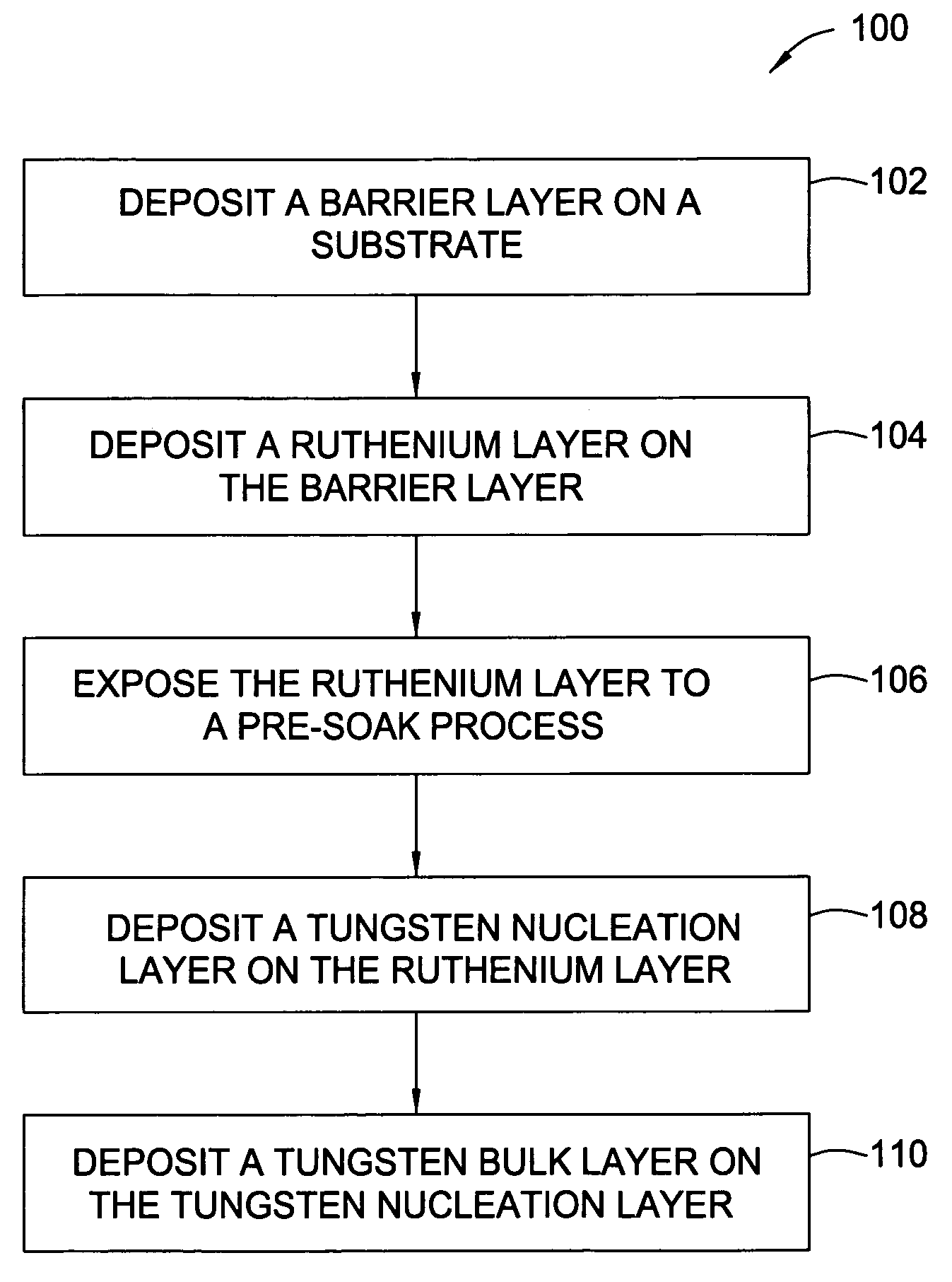
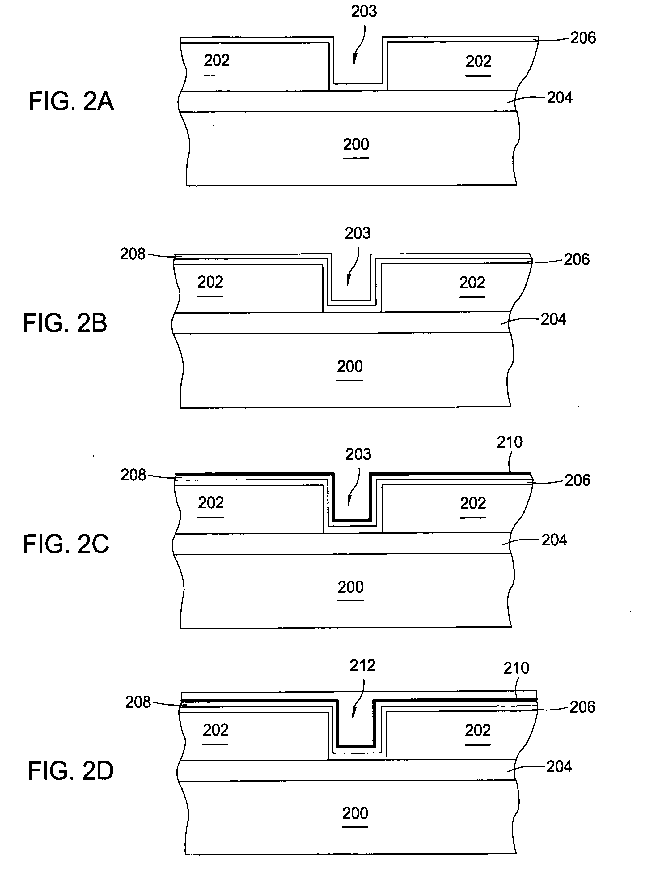
[0028] A method for depositing multiple layers of materials to form electronic devices is disclosed. Generally, the method includes depositing a barrier layer on a substrate surface, depositing a ruthenium layer on the barrier layer, depositing a tungsten nucleation layer on the ruthenium layer, and depositing a tungsten bulk layer on the tungsten nucleation layer. During the deposition of any of the aforementioned layers, the method may include a variety of deposition techniques including atomic layer deposition (ALD), chemical vapor deposition (CVD), physical vapor deposition (PVD), electrochemical plating (ECP) and / or electroless plating. Preferably, the method utilizes ALD processes to deposit the barrier layer, the ruthenium layer, the tungsten nucleation layer and the tungsten bulk layer. Also, a pre-soak process to nucleate an underlayer may be used prior to starting any of the deposition processes, for example, a ruthenium layer may be exposed to a pre-soak process that incl...


PUM

PropertyMeasurementUnit
Timeaaaaaaaaaa
Timeaaaaaaaaaa

Abstract

In one embodiment, a method for depositing a tungsten-containing film on a substrate is provided which includes depositing a barrier layer on the substrate, such as a titanium or tantalum containing barrier layer and depositing a ruthenium layer on the barrier layer. The method further includes depositing a tungsten nucleation layer on the ruthenium layer and depositing a tungsten bulk layer on the tungsten nucleation layer. The barrier layer, the ruthenium layer, the tungsten nucleation layer and the tungsten bulk layer are independently deposited by an ALD process, a CVD process or a PVD process, preferably by an ALD process. In some examples, the substrate is exposed to a soak process prior to depositing a subsequent layer, such as between the deposition of the barrier layer and the ruthenium layer, the ruthenium layer and the tungsten nucleation layer or the tungsten nucleation layer and the tungsten bulk layer.

Description

BACKGROUND OF THE INVENTION [0001] 1. Field of the Invention [0002] Embodiments of the present invention generally relate to methods for barrier layer, ruthenium layer and tungsten layer formation and, more particularly to ruthenium deposition processes for use in tungsten integration. [0003] 2. Description of the Related Art [0004] Sub-quarter micron multilevel metallization is one of the key technologies for the next generation of very large scale integration (VLSI). The multilevel interconnects that lie at the heart of this technology possess high aspect ratio features, including contacts, vias, lines, or other apertures. Reliable formation of these features is very important to the success of VLSI and to the continued effort to increase quality and circuit density on individual substrates. Therefore, there is a great amount of ongoing effort being directed to the formation of void-free features having high aspect ratios of 10:1 (height:width) or greater. [0005] Tungsten, replaci...

Claims


Application Information

Patent Timeline
IPC IPC(8): H01L21/44
CPCC23C16/0281Y10T428/12771C23C16/45525C23C16/45529H01L21/28556H01L21/28562H01L21/76843H01L21/76846H01L21/76862H01L21/76876H01L21/76877Y10T428/12812Y10T428/12875Y10T428/12861C23C16/06
Inventor GANDIKOTA, SRINIVASMOORTHY, MADHUKHANDELWAL, AMITGELATOS, AVGERINOS V.CHANG, MEISHAH, KAVITAGANGULI, SESHADRI
Owner APPLIED MATERIALS INC
Why Eureka
Try Eureka