Polishing pad for semiconductor wafer and laminated body for polishing of semiconductor wafer equipped with the same as well as method for polishing of semiconductor wafer

Active Publication Date: 2006-06-15
JSR CORPORATIOON
View PDF9 Cites 40 Cited by
  • Summary
  • Abstract
  • Description
  • Claims
  • Application Information

AI Technical Summary

Benefits of technology

[0005] The present invention is to solve the above-mentioned problems and an objective of the present invention is to provide a polishing pad for a semiconductor wafer through which can transmit endpoint detecting light without lowering polishing performance, u

Problems solved by technology

However, since the window in the above-mentioned polishing pad has substantially no ability to retain and discharge the slurry, there is a possibility that provision of a window decreases the polishing a

Method used


Image

  • Polishing pad for semiconductor wafer and laminated body for polishing of semiconductor wafer equipped with the same as well as method for polishing of semiconductor wafer
  • Polishing pad for semiconductor wafer and laminated body for polishing of semiconductor wafer equipped with the same as well as method for polishing of semiconductor wafer
  • Polishing pad for semiconductor wafer and laminated body for polishing of semiconductor wafer equipped with the same as well as method for polishing of semiconductor wafer

Examples


Embodiment Construction

[0012] The present invention will be explained in detail below.

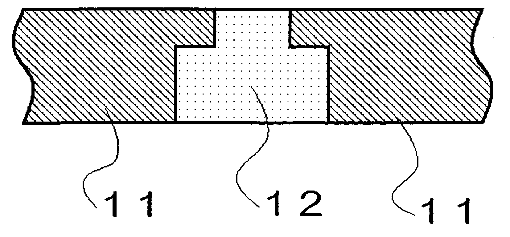
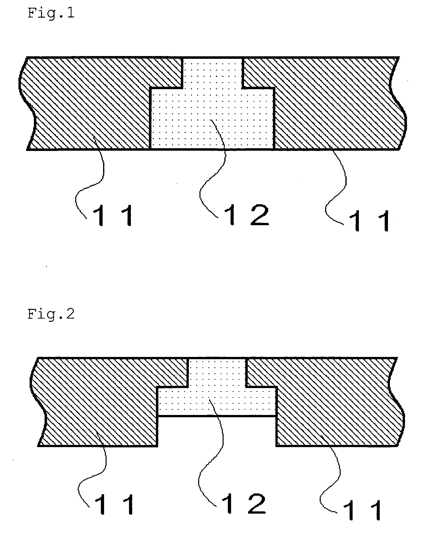
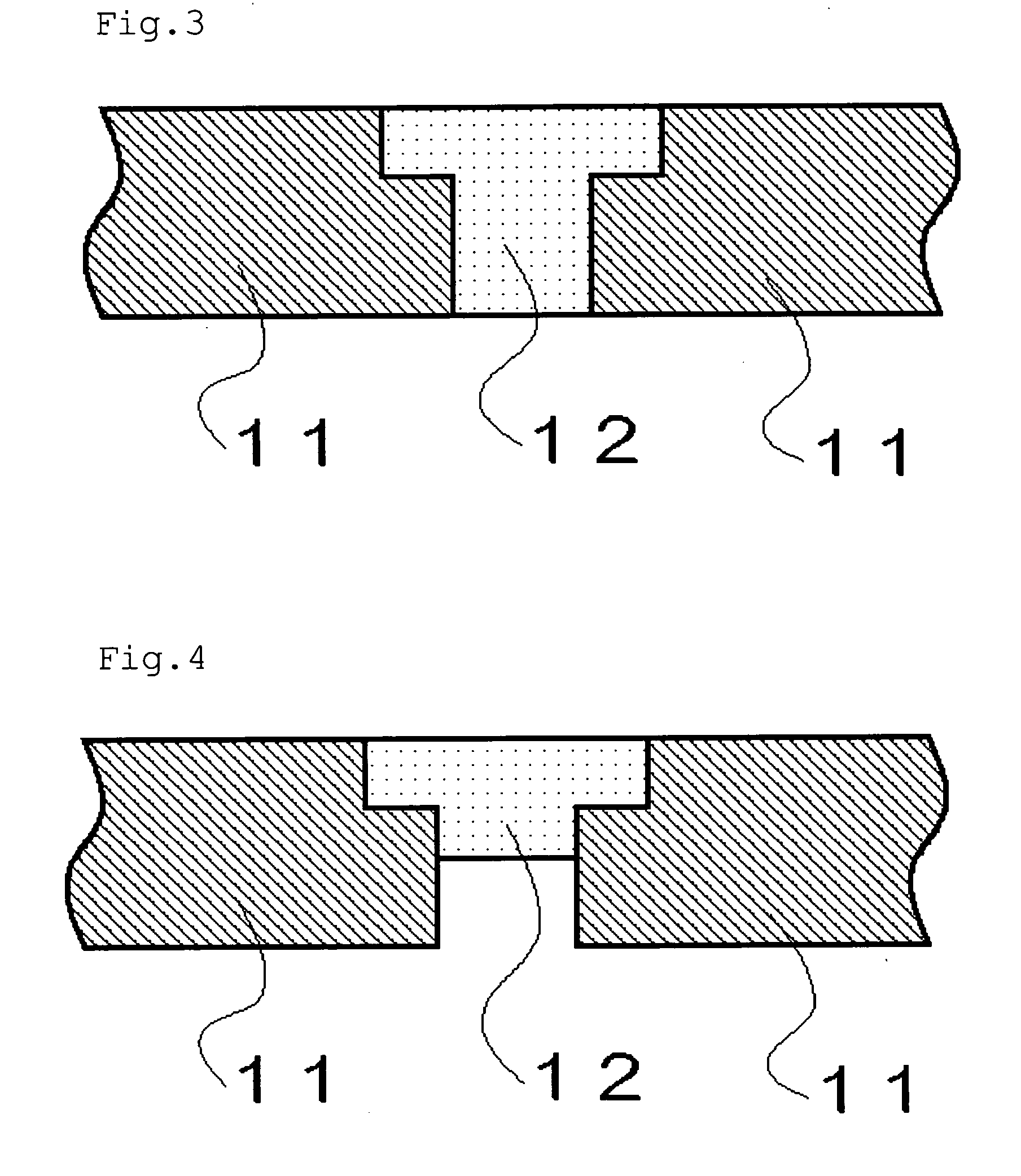
[0013] The polishing pad for a semiconductor wafer (hereinafter also referred to as “polishing pad”) of the present invention is characterized in that it comprises a substrate for a polishing pad provided with a through hole penetrating from surface to back, and a light transmitting part fitted in the through hole, wherein the light transmitting part comprises a water-insoluble matrix material and a water-soluble particle dispersed in the water-insoluble matrix material, and wherein a content of the water-soluble particle is not less than 0.1% by volume and less than 5% by volume based on 100% by volume of the total amount of the water-insoluble matrix material and the water-soluble particle.

[0014] The “substrate for a polishing pad” can usually retain the slurry on the surface thereof and, further, make wastages reside transiently. The transmitting properties of this substrate for a polishing pad may be present or abs...


PUM

PropertyMeasurementUnit
Percent by volumeaaaaaaaaaa

Abstract

An objective of the present invention is to provide a polishing pad for a semiconductor wafer and a laminated body for polishing of a semiconductor wafer equipped with the same which can perform optical endpoint detection without lowering the polishing performance as well as methods for polishing of a semiconductor wafer using them. The polishing pad of the present invention comprises a substrate 11 for a polishing pad provided with a through hole penetrating from surface to back, a light transmitting part 12 fitted in the through hole, the light transmitting part comprises a water-insoluble matrix material (1,2-polybutadiene) and a water-soluble particle (β-cyclodextrin) dispersed in the water-insoluble matrix material, and the water-soluble particle is less than 5% by volume based on 100% by volume of the total amount of the water-insoluble matrix material and the water-soluble particle. In addition, the laminated body for polishing of the present invention comprises a supporting layer on a backside of the polishing pad. These polishing pad and laminated body for polishing can comprise a fixing layer 13 on a backside.

Description

TECHNICAL FIELD [0001] The present invention relates to a polishing pad for a semiconductor wafer and a laminated body for polishing of a semiconductor wafer equipped with the same as well as methods for polishing of a semiconductor wafer. More particularly, the present, invention relates to a polishing pad for a semiconductor wafer through which can transmit the light without decreasing the polishing performance, and a laminated body for polishing of a semiconductor wafer equipped with the same as well as methods for polishing of a semiconductor wafer. The polishing pad for a semiconductor wafer, and a laminated body for polishing of a semiconductor wafer equipped with the same, as well as methods for polishing of a semiconductor wafer of the present invention are suitable as a method for performing polishing of a semiconductor wafer or the like while polishing state is observed using an optical endpoint detecting apparatus. BACKGROUND TECHNOLOGY [0002] In polishing of a semiconduc...

Claims


Application Information

Patent Timeline
IPC IPC(8): B24B49/00B24B1/00B24B7/30B24B37/20B24D7/12B24D13/14H01L21/304
CPCB24B37/205
Inventor SHIHO, HIROSHIHOSAKA, YUKIOHASEGAWA, KUOKAWAHASHI, NOBUO
Owner JSR CORPORATIOON
Why Eureka
Try Eureka