Purged vacuum chuck with proximity pins

a vacuum chuck and proximity pin technology, applied in the field of vacuum chuck with proximity pins, can solve the problems of particulate contaminants entering the process environment, defects in the circuitry fabricated on the substrate, etc., and achieve the effects of reducing the time of substrate transition, reducing the proximity of height, and increasing the thermal transfer rate of energy

Inactive Publication Date: 2006-06-22
SOKUDO CO LTD
View PDF7 Cites 427 Cited by
  • Summary
  • Abstract
  • Description
  • Claims
  • Application Information

AI Technical Summary

Benefits of technology

[0010] Many benefits are achieved by way of the present invention over conventional techniques. For example, the present technique reduces the number of particles generated by contact between the backside surface of the substrate and the support plate. Moreover, embodiments of the present invention provide reduced height proximity pins while controlling the pin height to within a desired tolerance. The reduction in proximity pin height increases the thermal transfer rate of energy from the substrate to the plate assembly, thereby decreasing the time the substrate spends transitioning to a final temperature, increasing system throughput. Moreover, in some embodiments, an increase in thermal coupling between the substrate and plate assembly results in improvements in the thermally depende

Problems solved by technology

During substrate processing, the chuck material can abrade the material present on the underside of the substrate, resulting in the introduction of particulate contaminants to the process environment.
Consequently,

Method used


Image

  • Purged vacuum chuck with proximity pins
  • Purged vacuum chuck with proximity pins
  • Purged vacuum chuck with proximity pins

Examples


Embodiment Construction

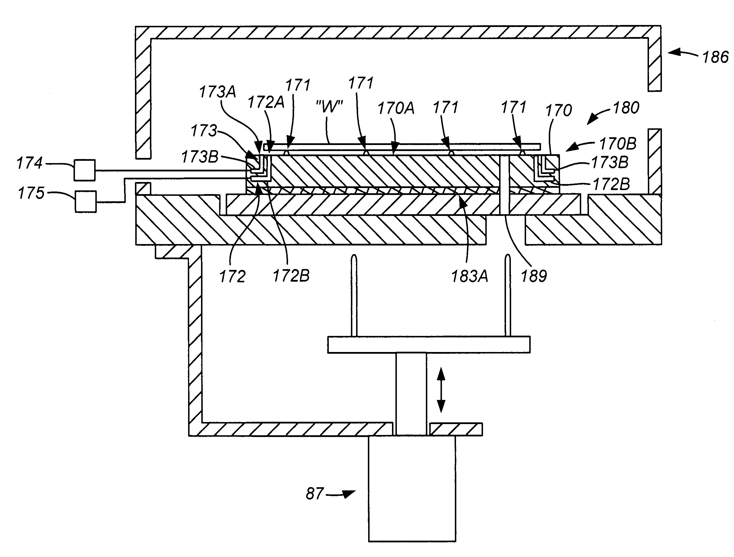
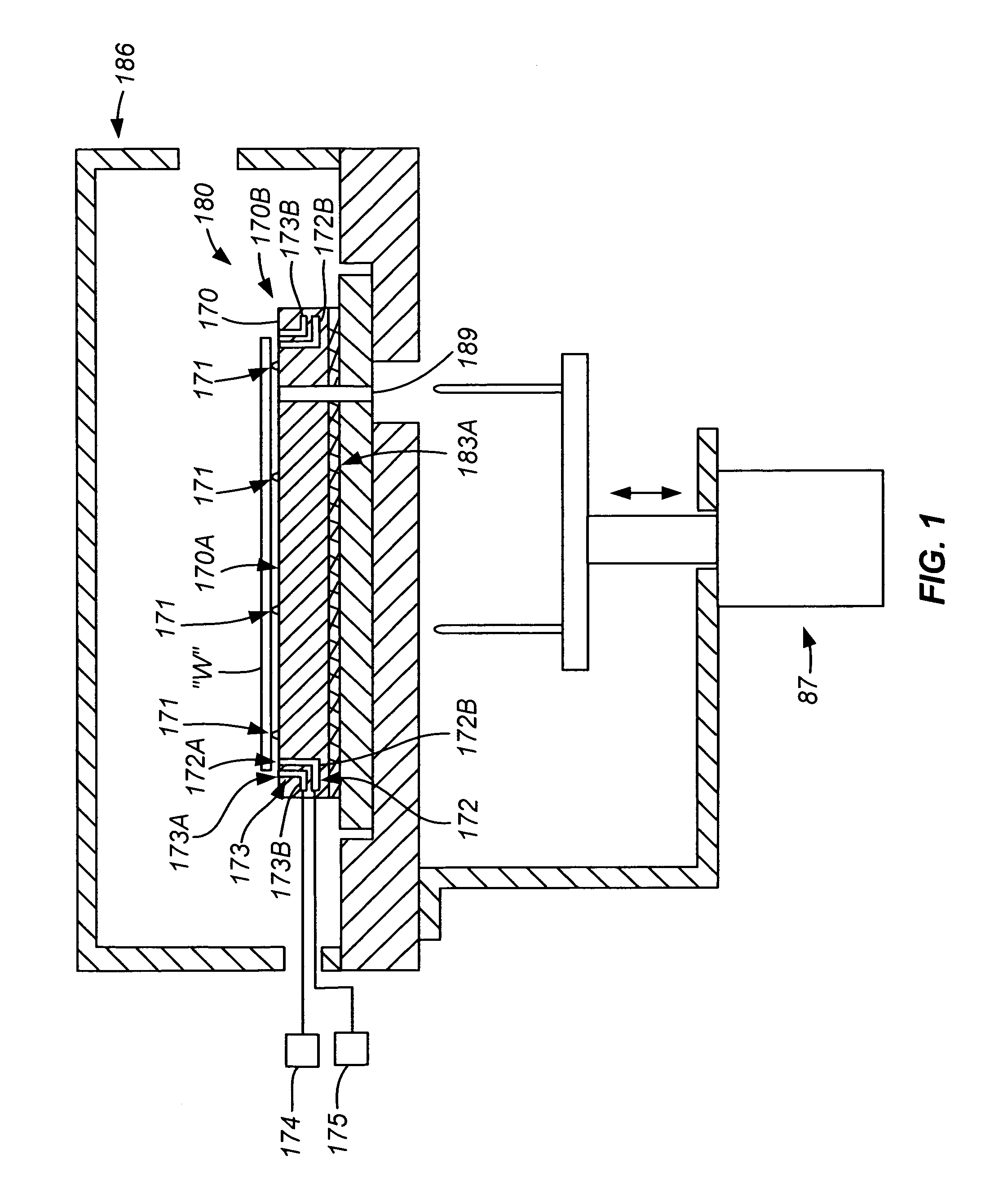
[0021] According to the present invention, methods and apparatus related to semiconductor manufacturing equipment are provided. More particularly, embodiments of the present invention relate to a method and apparatus for supporting a substrate during semiconductor processing operations. The method and apparatus can be applied to electrostatic chucks, vacuum chucks, and other applications as well.

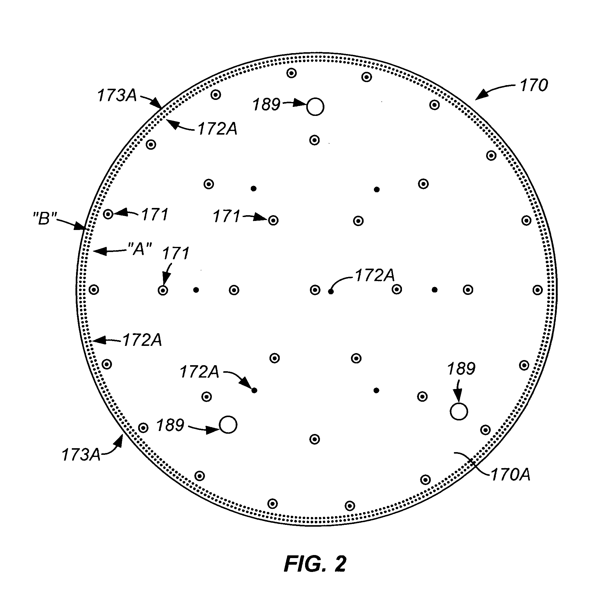
[0022]FIG. 1 is a simplified schematic side view illustration of a substrate processing chamber according to one embodiment of the present invention. In the embodiment illustrated in FIG. 1, the assembly 180 contains a plate assembly 170 and a vacuum source 175, which are mounted in a processing module 186. The plate assembly 170 generally contains a plate 170B, plate assembly surface 170A, protrusions 171, and a vacuum source port assembly 172. In this configuration the vacuum source 175 is used to create a negative pressure in the vacuum port plenum 172B, thus causing air to flow into a n...


PUM

PropertyMeasurementUnit
Thicknessaaaaaaaaaa
Diameteraaaaaaaaaa
Depthaaaaaaaaaa

Abstract

A substrate support structure comprising a first surface and a second surface opposite the first surface. The substrate support structure also comprises a plurality of proximity pins projecting to a first height above the first surface, the first height being less than 100 μm. In addition, the substrate support structure further comprises a plurality of purge ports passing from the second surface to the first surface and a plurality of vacuum ports passing from the second surface to the first surface. In one embodiment, the plurality of purge ports are arranged in a first circular pattern, the first circular pattern having a first radial dimension less than the radius of the substrate support, and the plurality of vacuum ports are arranged in a second circular pattern, the second circular pattern having a second radial dimension less than the first radial dimension.

Description

CROSS-REFERENCES TO RELATED APPLICATIONS [0001] This application claims the benefit of U.S. Provisional Application Ser. No. 60 / 639,109, filed Dec. 22, 2004, entitled “Twin Architecture For Processing A Substrate,” which is incorporated herein by reference.BACKGROUND OF THE INVENTION [0002] The present invention relates generally to the field of semiconductor processing equipment. More particularly, the present invention relates to a method and apparatus for supporting a substrate inside a semiconductor processing chamber. The method and apparatus can be applied to electrostatic chucks, vacuum chucks, and other applications as well. [0003] Substrate support chucks are widely used to support substrates within semiconductor processing systems. Two examples of particular types of chucks used in semiconductor processing systems include electrostatic chucks (e-chucks) and vacuum chucks. These chucks are used to retain semiconductor wafers, or other workpieces, in a stationary position du...

Claims


Application Information

Patent Timeline
IPC IPC(8): H01L21/306C23C16/00
CPCH01L21/67173H01L21/67745H01L22/26H01L21/67196H01L21/6831G03B27/32Y10S414/136H01L21/67109H01L21/68707H01L21/67742H01L21/6719G03F7/40Y10T29/53187H01L21/67161Y10S414/135H01L21/67754H01L21/67178G03D13/006H01L21/67748G05B2219/40476Y10T29/5323G05B19/41825H01L21/67184G05B2219/49137H01L21/6838H01L21/6715G05B2219/45031H01L21/67225Y02P90/02
Inventor HERCHEN, HARALD
Owner SOKUDO CO LTD
Why Eureka
Try Eureka