Organic light-emitting device with improved layer structure

Active Publication Date: 2006-06-22
CHINA STAR OPTOELECTRONICS INT HK
View PDF42 Cites 56 Cited by
  • Summary
  • Abstract
  • Description
  • Claims
  • Application Information

AI Technical Summary

Benefits of technology

[0021] The second aspect of the present invention provides a method of improving a process for fabricating an organic light emitting device, the device comprising a cathode, an anode, and an organic layer structure disposed between the cathode and the anode, the org

Problems solved by technology

In the fabrication of a full-color organic display device,

Method used


Image

  • Organic light-emitting device with improved layer structure
  • Organic light-emitting device with improved layer structure
  • Organic light-emitting device with improved layer structure

Examples


Embodiment Construction

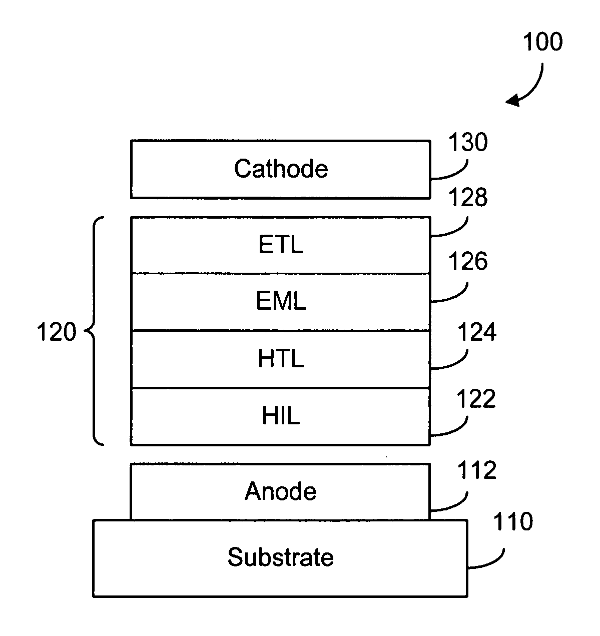
[0056] The structure of the organic light-emitting device (OLED), according to the present invention, is shown in FIG. 2. In general, the OLED 100 comprises an organic layer structure 120 disposed between an anode layer 112 and a cathode layer 130. The anode layer 112 is disposed on a substrate 110. The organic layer structure 120 may comprise a hole injection layer (HIL) 122, a hole transport layer (HTL) 124, an emissive layer (EML) 126 and an electron transport layer (ETL) 128. The organic layer structure 120, according to the present invention, comprises substantially an organic host material for use in the HIL 122, the HTL 124, the EML 126 and the ETL 128. As shown in FIGS. 3a and 3b, the organic host material in the HIL 122 is doped with a p-type dopant; the organic host material in the EML 126 is doped with a luminescent dopant or dye; and the organic host material in the ETL 128 is doped with an n-type dopant. The luminescent dopant in the EML 126 can be a fluorescent dopant ...


PUM

PropertyMeasurementUnit
Structureaaaaaaaaaa
Transport propertiesaaaaaaaaaa
Fluorescenceaaaaaaaaaa

Abstract

An organic light emitting device having a cathode, an anode and an organic layer structure disposed between the cathode and the anode, the organic layer structure comprising a hole injection layer doped with a p-type dopant, a hole transport layer, an emissive layer and an electron transport layer doped with an n-type dopant, wherein all of the layers in the organic layer structure are substantially made from the same organic host material. In particular, the organic host material is a bipolar organic material such as a derivative of fused aromatic rings. The emissive layer can be doped with a fluorescent dye or a phosphorescent dye.

Description

FIELD OF THE INVENTION [0001] The present invention relates generally to light-emitting devices and, more particularly, to organic light-emitting diodes. BACKGROUND OF THE INVENTION [0002] Organic light-emitting diodes OLEDs are known in the art. For example, Kido et al. (U.S. Pat. No. 6,013,384) discloses, as shown in FIG. 1a, an organic electroluminescent device 10 wherein the organic layers consist of a hole transport layer (HTL) 13, an emissive layer 14 and a metal-doped organic compound layer 15 disposed between an anode layer 12 and a cathode layer 16. The device is fabricated on a substrate 11. According to Kido et al., the organic compounds which can be used in the formation of the emissive layer, the electron transport layer and the metal-doped layer in the OLED device, include polycyclic compounds, condensed polycyclic hydrocarbon compounds, condensed heterocyclic compounds, etc. The dopant in the metal-doped organic compound layer is a metal having a work function of less...

Claims


Application Information

Patent Timeline
IPC IPC(8): H01L29/08H01L35/24H01L51/00H01L51/30H01L51/50H05B33/12
CPCH01L51/002H01L51/0052H01L51/5012H01L51/5052H10K71/30H10K85/615H10K50/155H10K50/165H10K50/11
Inventor LI, SHI-HAO
Owner CHINA STAR OPTOELECTRONICS INT HK
Why Eureka
Try Eureka