

Device having an organic transistor integrated with an organic light-emitting diode's heterojunctions
- Summary
- Abstract
- Description
- Claims
- Application Information
AI Technical Summary
Benefits of technology
Problems solved by technology
Method used
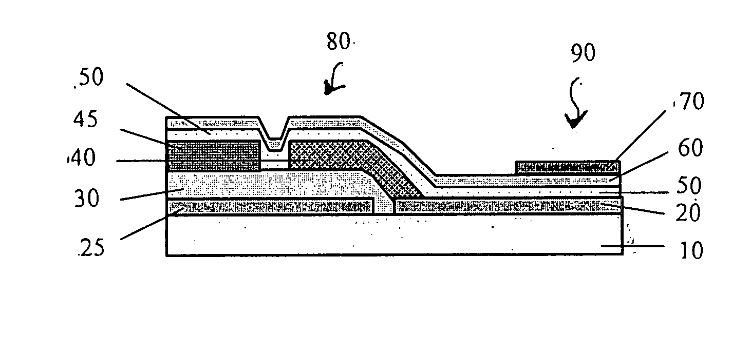
Image

Examples
Embodiment Construction
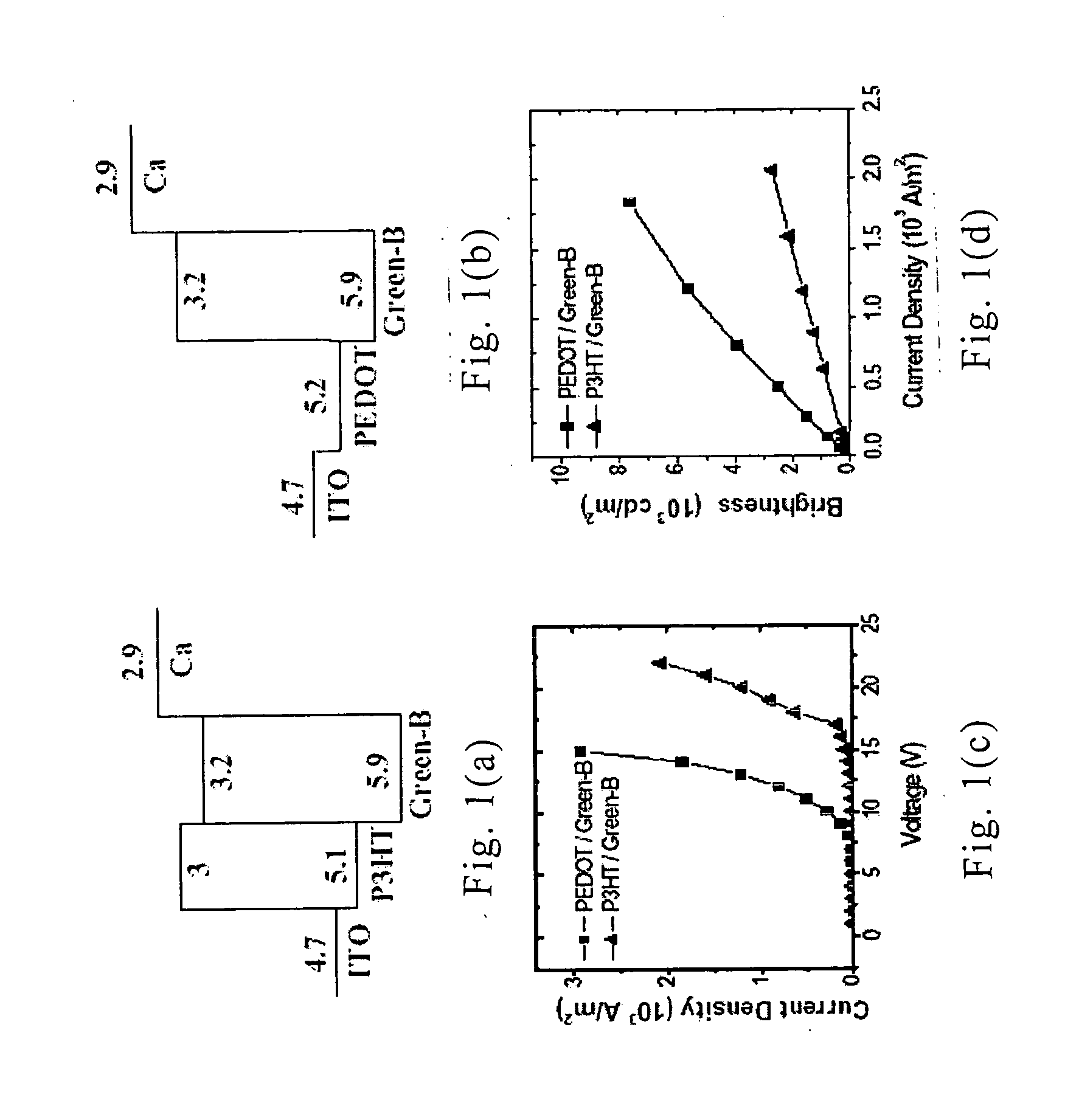
[0028]FIGS. 1a and 1b are structural energy band graphs of organic heterojunction light-emitting diodes according to a preferred embodiment of the present invention. FIGS. 1c and 1d are comparative graphs of organic light-emitting diodes which uses poly ethylenedioxythiophene (PEDOT serving as hole transport layers (HTLs) thereof according to a preferred embodiment of the present invention. Please referring to FIGS. 1a, 1b, 1c, and 1d simultaneously, in the organic light-emitting diode structure using PEDOT as a hole transport layer, the thickness of an organic light-emitting layer can be controlled. When the organic light-emitting layer is thick, the body is much superior to the heterojunction in light emission so as to make the entire color of light close to the color of light emitted from the organic light-emitting layer. When the organic light-emitting layer is thin, the heterojunction is superior to the body in light emission, and an exciplex can be used to generate required co...
PUM
| Property | Measurement | Unit |
|---|---|---|
| Color | aaaaa | aaaaa |
| Efficiency | aaaaa | aaaaa |
| Transparency | aaaaa | aaaaa |
Abstract
Description
Claims
Application Information