Curable material and its application

a technology of curable materials and conductive materials, applied in the field of curable materials, can solve the problems of reducing the luminous efficiency of organic light emitting diodes, the difference in energy level between the hole transporting layer material and the emitting material is too large, and the hole transporting ability of most blue or green luminescent materials is poor

Active Publication Date: 2013-11-12
ETERNAL MATERIALS CO LTD
View PDF4 Cites 2 Cited by
  • Summary
  • Abstract
  • Description
  • Claims
  • Application Information

AI Technical Summary

Benefits of technology

[0018]The curable material of the present invention can generate crosslinking structure by heating and then be cured. The solubility of the cured product in common organic solvents is greatly reduced, and therefore, the problem of poor luminous efficiency due to the dissolution of the hole transporting layer material in a solvent occurred in the prior art can be solved. Furthermore, the present invention allows the energy level of the curable material of the present invention to be closer to the species of the luminescent material by combining the corresponding luminescent material and adjusting the component ratio. The problem of mismatching the energy level between the hole transporting layer material and the luminescent material (such as blue or green light) in the known organic electroluminescent device then can be solved and the luminous efficiency of the organic electroluminescent device is improved.
[0018]The curable material of the present invention can generate crosslinking structure by heating and then be cured. The solubility of the cured product in common organic solvents is greatly reduced, and therefore, the problem of poor luminous efficiency due to the dissolution of the hole transporting layer material in a solvent occurred in the prior art can be solved. Furthermore, the present invention allows the energy level of the curable material of the present invention to be closer to the species of the luminescent material by combining the corresponding luminescent material and adjusting the component ratio. The problem of mismatching the energy level between the hole transporting layer material and the luminescent material (such as blue or green light) in the known organic electroluminescent device then can be solved and the luminous efficiency of the organic electroluminescent device is improved.
[0018]The curable material of the present invention can generate crosslinking structure by heating and then be cured. The solubility of the cured product in common organic solvents is greatly reduced, and therefore, the problem of poor luminous efficiency due to the dissolution of the hole transporting layer material in a solvent occurred in the prior art can be solved. Furthermore, the present invention allows the energy level of the curable material of the present invention to be closer to the species of the luminescent material by combining the corresponding luminescent material and adjusting the component ratio. The problem of mismatching the energy level between the hole transporting layer material and the luminescent material (such as blue or green light) in the known organic electroluminescent device then can be solved and the luminous efficiency of the organic electroluminescent device is improved.
[0014]The detailed technology and preferred embodiments implemented for the subject invention are described in the following paragraphs for people skilled in this field to well appreciate the above objectives, technical features and advantages of the claimed invention.

Problems solved by technology

Commonly used hole transporting layer materials have some obvious disadvantages, such as poor hole transporting ability for most of the blue or green luminescent materials due to mismatched energy levels; i.e., the difference in energy level between the hole transporting layer material and emitting material is too great.
In addition, exciton quenching easily occurs at the interface between the luminescent material and hole transporting layer material, thus, reducing the luminous efficiency of the organic light emitting diode.
The structure of the underlying hole transporting layer can be easily damaged (for example, generating an uneven surface, increasing roughness or producing pores) while spin coating the emitting layer because the hole transporting layer material has insufficient organic solvent resistance.
This would impede the combination between electrons and holes, then, further affecting the luminous efficiency of the organic light emitting diodes.

Method used


Image

  • Curable material and its application
  • Curable material and its application
  • Curable material and its application

Examples


example 1

The Preparation of Curable Material

[0045][The Preparation of Curable Material 1]

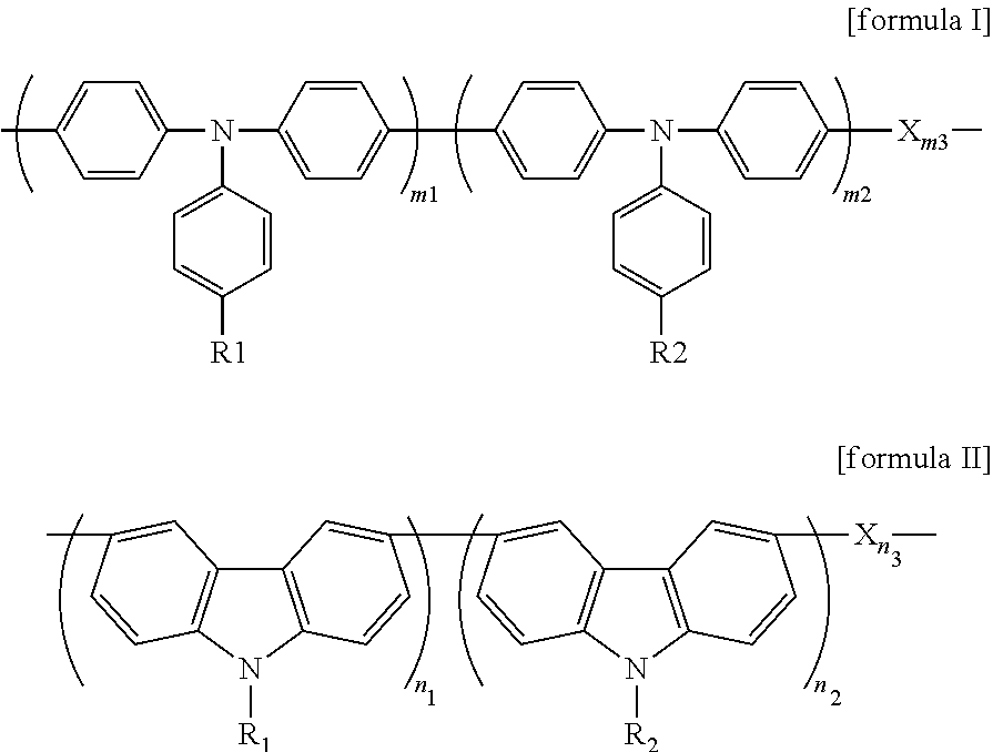
[0046]First, N,N-bis(4-bromophenyl)-p-(4-vinylphenyl)aniline (3) was synthesized. Tri(4-bromophenyl)amine (1) and p-vinylphenyl boric acid (2) with a molar ratio of about 2:1 and zero valence palladium compound (PPh3)4Pd(0) as a catalyst in a suitable amount were dissolved in a mixture solution consisting of tetrahydrofuran (about 20 mL) and 2M potassium phosphate aqueous solution (about 11 mL). The resulting mixture was first purged with argon and vigorously stirred at about 100° C. and reacted for about 48 hours. The reaction scheme is as follows:

[0047]

[0048]The obtained mixture after reaction was poured into 50 mL water and extracted with dichloromethane (about 250 mL) twice. The combined organic extracts were dried by anhydrous magnesium sulfate and further concentrated by rotary evaporation. Further purification by silica gel column chromatography (ethyl acetate / n-hexane) afforded N,N-bis(4-bromophe...

example 2

Luminous Efficiency Test

[0066][OLED 1]

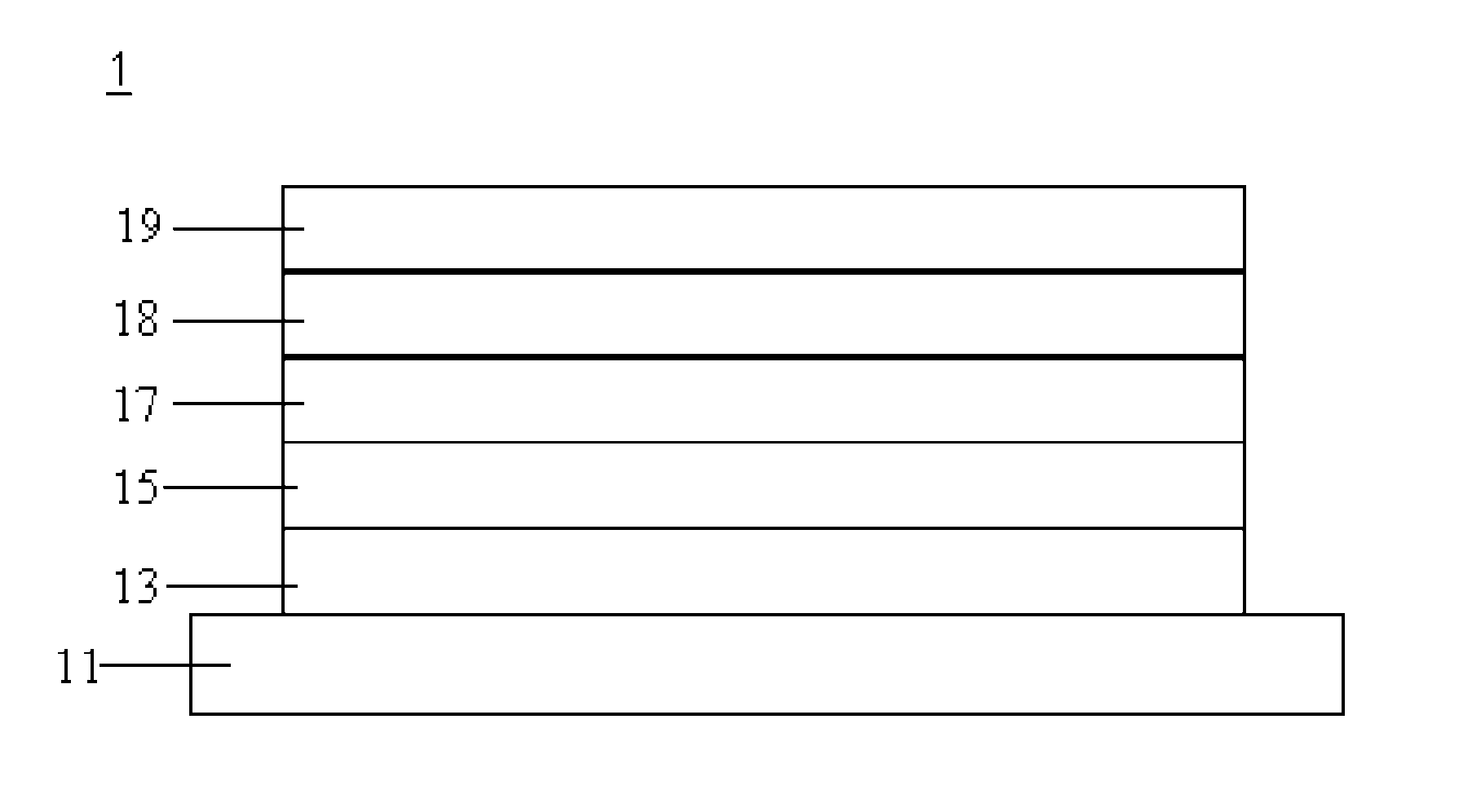
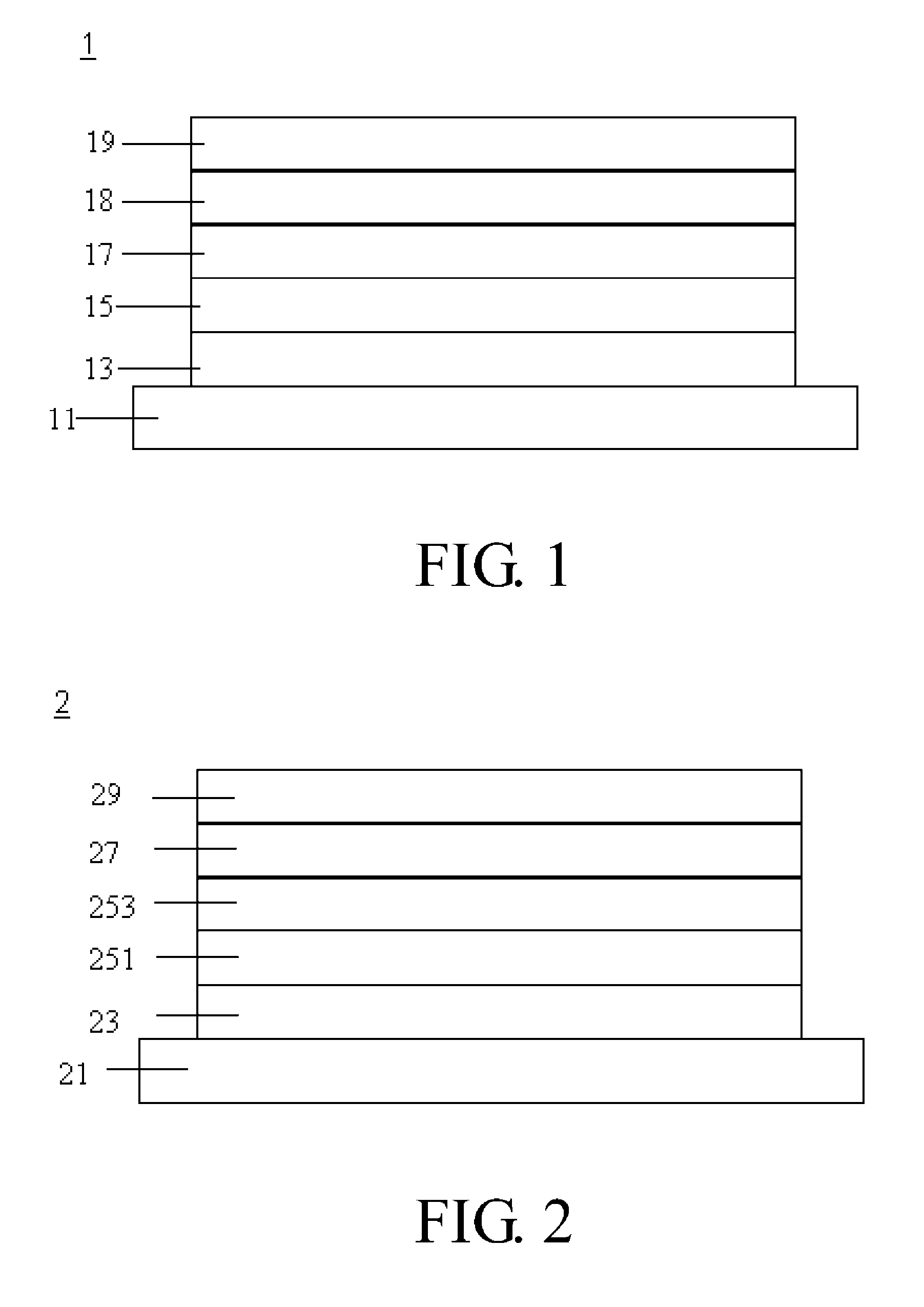
[0067]The curable material 1 of the present invention was used as a hole transporting layer material to fabricate OLED 1 with a structure as shown in FIG. 2. In particular, an ITO layer was deposited on a glass substrate as an anode. The ITO-coated glass substrate was washed via ultrasonic bath and further treated in a UV-ozone chamber. A PEDOT: PSS layer was spin-coated on the top of the anode and annealed at about 150° C. for about 15 minutes. Then, a toluene solution of the curable material 1 of the present invention was spin-coated on the top of the PEDOT: PSS layer (about 10 mg / mL; about 2000 rpm) and thermally treated at about 230° C. for about 30 minutes under nitrogen atmosphere to cure the curable material 1 to form a hole transporting layer (about 40 nm). Poly(9,9-dioctylfluorene) was then spin-coated on the top of the hole transporting layer as an emitting layer (about 70 nm). Finally, a thin cathode layer was deposited by successive ...


PUM

PropertyMeasurementUnit
structureaaaaaaaaaa
luminescentaaaaaaaaaa
electroluminescentaaaaaaaaaa

Abstract

A curable material is provided. The curable material has the structure of formula I or formula II:wherein, X, R1, R2, m1 to m3, and n1 to n3 are defined as cited in the description.

Description

CROSS REFERENCE[0001]This application claims the benefit of Taiwan Patent Application No. 100103891, filed on Feb. 1, 2011 in the Taiwan Intellectual Property Office, the disclosure of which is incorporated herein in its entirety by reference.BACKGROUND[0002]1. Field of the Invention[0003]The present invention relates to a curable material. In particular, the present invention relates to a curable material that can be used in an organic electroluminescent device as a hole transporting layer material.[0004]2. Descriptions of the Related Art[0005]The organic electroluminescent phenomenon was firstly observed and studied in the 1960s (E. Gurnee et al., U.S. Pat. No. 3,172,862 (1965)). Kodark Company (US) invented an organic light emitting diode (OLED) in the 1980s and used the vapor deposition method to prepare a double layer structure of organic films (C. W. Tang, U.S. Pat. No. 4,356,429 (1987), and C. W. Tang et al., Appl. Phys. Lett. 51, 12:913 (1987)). Since then, studies of organi...

Claims


Application Information

Patent Timeline
Patent Type & Authority Patents(United States)
IPC IPC(8): H01L51/54
CPCC09K11/06H01L51/0035H01L51/0043H05B33/14C08G61/12C08G61/124C09K2211/1416C09K2211/1425C09K2211/1433C09K2211/1466H01L51/5056C08G2261/135C08G2261/1414C08G2261/3142C08G2261/3162C08G2261/3241C08G2261/411C08G2261/512C08G2261/74C08G2261/76C08G2261/95H10K85/111H10K85/151H10K50/15
Inventor CHEN, SHINN-HORNGCHEN, RUEI-TANGSU, CHE-WEI
Owner ETERNAL MATERIALS CO LTD
Why Eureka
Try Eureka