Light transmitting window member, semiconductor package provided with light transmitting window member and method for manufacturing light transmitting window member

a technology of semiconductor packages and light transmission windows, which is applied in the direction of semiconductor/solid-state device details, optical radiation measurement, instruments, etc., can solve the problems of difficult to simplify the structure and manufacturing steps of conventional light transmission windows, and increase the material cost of the frame b>22/b>, so as to simplify the polishing step of the glass member and reduce the thickness of the frame. , the effect of easy polishing

Inactive Publication Date: 2006-06-22
NEOMAX MATERIALS
View PDF2 Cites 52 Cited by
  • Summary
  • Abstract
  • Description
  • Claims
  • Application Information

AI Technical Summary

Benefits of technology

[0010] The present invention has been proposed in order to solve the aforementioned problems, and an object of the present invention is to provide a light transmission window member capable of simplifying the structure and capable of simplifying manufacturing steps, a semiconductor package comprising a light transmission window member and a method of manufacturing a light transmission window member.

Problems solved by technology

On that account, there is such a problem that the material cost for the frame 22 is increased as compared with a case where the thickness of the frame 22 is small and it is difficult to simplify the structure of the light transmission window member 40 due to the large thickness of the frame 22.
In the structure disclosed in the aforementioned Japanese Patent Laying-Open No. 9-148469, the opening region (opening) for defining the light passage region is provided also on the glass member in addition to the provision of the opening on the frame, and hence there is such a problem that it is difficult to simplify the structure and manufacturing steps similarly to the conventional light transmission window member 40 shown in FIGS.

Method used


Image

  • Light transmitting window member, semiconductor package provided with light transmitting window member and method for manufacturing light transmitting window member
  • Light transmitting window member, semiconductor package provided with light transmitting window member and method for manufacturing light transmitting window member
  • Light transmitting window member, semiconductor package provided with light transmitting window member and method for manufacturing light transmitting window member

Examples


first embodiment

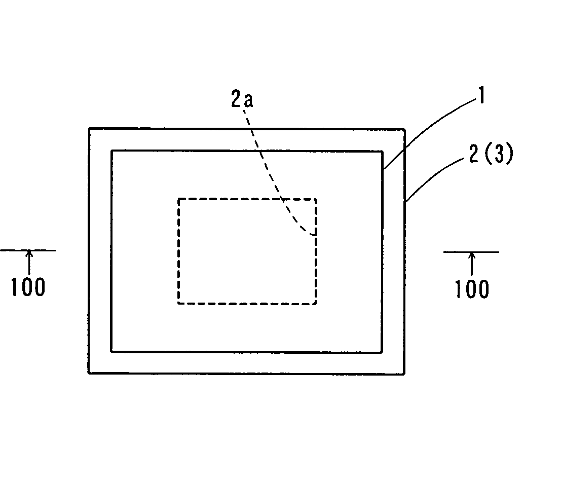
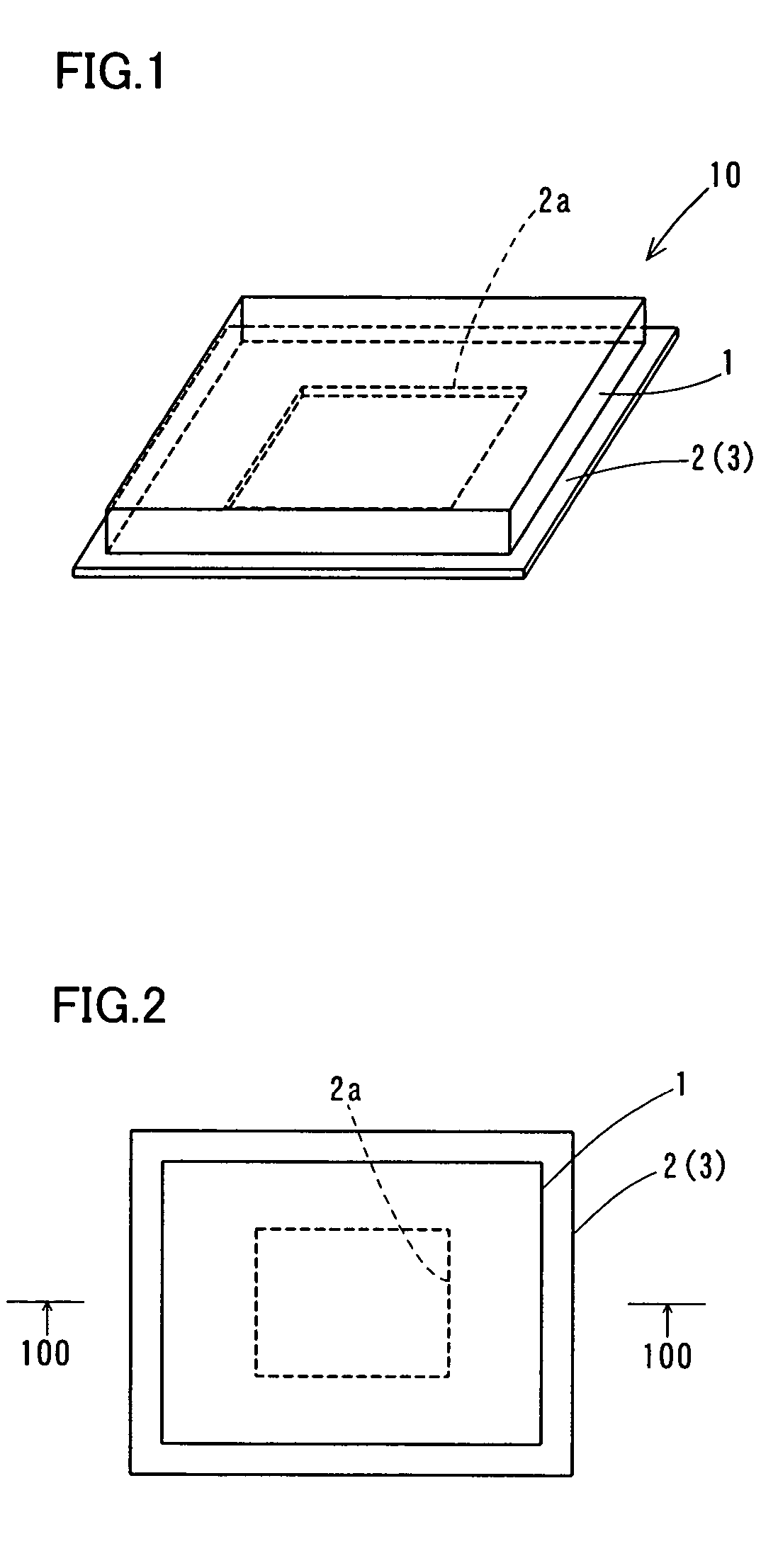
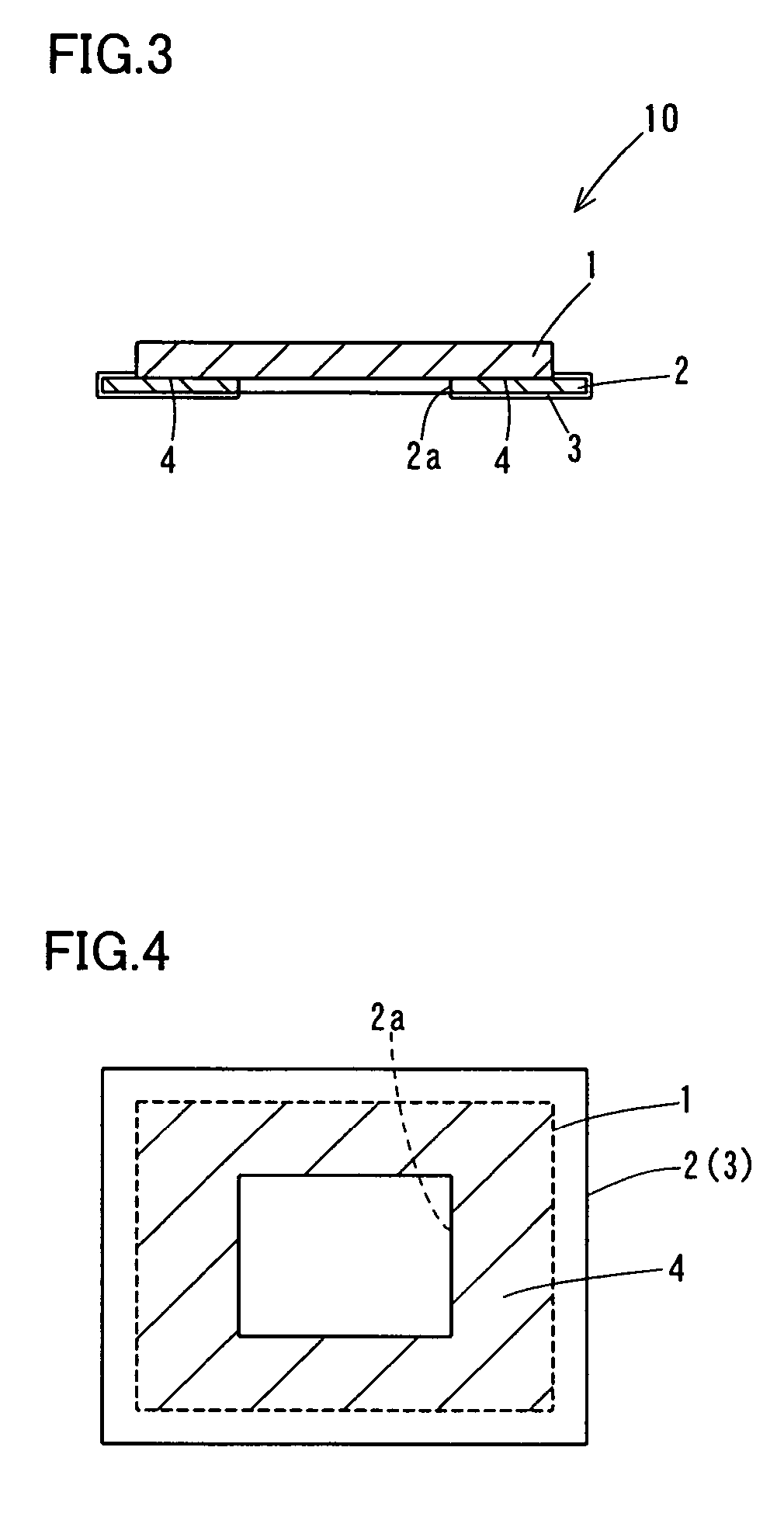
[0059] FIGS. 1 to 4 are diagrams showing the overall structure of a light transmission window member according to a first embodiment of the present invention. FIG. 5 is a perspective view for illustrating a manufacturing step for the light transmission window member according to the first embodiment of the present invention. FIG. 6 is a perspective view showing the overall structure of a semiconductor package comprising the light transmission window member shown in FIG. 1, and FIG. 7 is a perspective view for illustrating a manufacturing step for the semiconductor package shown in FIG. 6. The structures of a light transmission window member 10 according to the first embodiment of the present invention and a semiconductor package 30 comprising the light transmission window 10 are first described with reference to FIGS. 1 to 4 and 6.

[0060] The light transmission window member 10 according to the first embodiment of the present invention comprises a glass member 1 capable of transmitt...

second embodiment

[0070] FIGS. 8 to 11 are diagrams showing the overall structure of a light transmission window member according to a second embodiment of the present invention. FIG. 12 is a perspective view for illustrating a manufacturing step for the light transmission window member according to the second embodiment of the present invention. FIG. 13 is a perspective view showing the overall structure of a semiconductor package comprising the light transmission window member shown in FIG. 8. According to the second embodiment, a glass member 1 and a frame 2 of KOVAR are anodically bonded to each other through an Al layer 5, dissimilarly to the aforementioned first embodiment. The structures of a light transmission window member 10a according to the second embodiment of the present invention and a semiconductor package 30a comprising the light transmission window member 10a are now described with reference to FIGS. 8 to 11 and 13.

[0071] In the light transmission window member 10a according to the...


PUM


Abstract

A light transmission window member capable of simplifying the structure and capable of simplifying manufacturing steps is obtained. This light transmission window member (10, 10a), which is a light transmission window member employed for a semiconductor package (30, 30a), comprises a flat metal frame (2) having an opening (2a) for defining a light passage region and a glass member (1) capable of transmitting light bonded to the upper surface of the flat frame having the opening without through an adhesive to cover the opening.

Description

TECHNICAL FIELD [0001] The present invention relates to a light transmission window member, a semiconductor package comprising a light transmission window member and a method of manufacturing a light transmission window member, and more particularly, it relates to a light transmission window member including a glass member capable of transmitting light, a semiconductor package comprising a light transmission window member and a method of manufacturing a light transmission window member. BACKGROUND TECHNIQUE [0002] Various light transmission window members including glass members capable of transmitting light employed for semiconductor packages are known in general. For example, Japanese Patent Laying-Open No. 9-148469 discloses this type of light transmission window member. [0003] The aforementioned Japanese Patent Laying-Open No. 9-148469 discloses a light transmission window member having a structure obtained by forming an opening (opening region) for defining a light passage regi...

Claims


Application Information

Patent Timeline
Patent Type & Authority Applications(United States)
IPC IPC(8): H01L33/00G01J1/04H01L23/02H01L33/48
CPCG01J1/04G01J1/0407H01L31/0203H01L33/483
Inventor NAKAOKA, JUNICHIIKEUCHI, KENJITAKAHASHI, MAKOTO
Owner NEOMAX MATERIALS
Why Eureka
Try Eureka