Device using ambipolar transport in SB-MOSFET and method for operating the same

Inactive Publication Date: 2006-06-22
ELECTRONICS & TELECOMM RES INST
View PDF1 Cites 4 Cited by
  • Summary
  • Abstract
  • Description
  • Claims
  • Application Information

AI Technical Summary

Benefits of technology

[0022] According to the present invention, it is possible to provide a multi-bit memory and / or multi-bit logic device using a new characteristic of the SB-MOSFET.

Problems solved by technology

As the device is decreasing in size, many unexpected problems are rising.
A reduction of gate length inevitably causes short channel effect.
As size of devices becomes smaller, the devices following a simple electrical and physical law show complex characteristics caused by several new physical phenomena, which result from the short channel effect.
However, the top-down technique has a limitation in reducing the size of the device.
The major problem of these new electronic devices is that they are yet in development level and it is difficult to apply the existing advanced silicon (Si) processing technologies to them.

Method used


Image

  • Device using ambipolar transport in SB-MOSFET and method for operating the same
  • Device using ambipolar transport in SB-MOSFET and method for operating the same
  • Device using ambipolar transport in SB-MOSFET and method for operating the same

Examples


Embodiment Construction

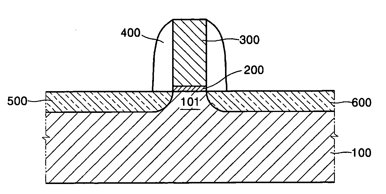
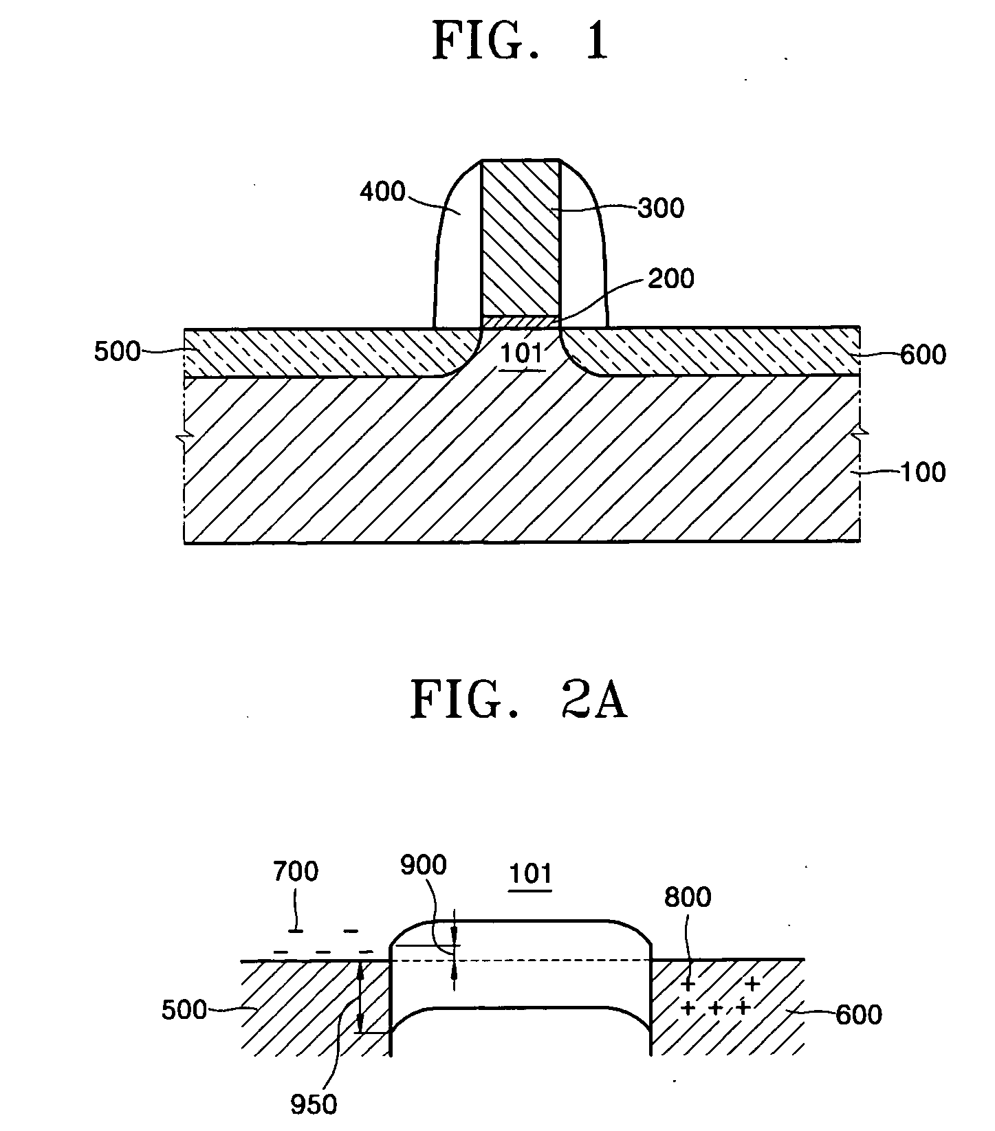
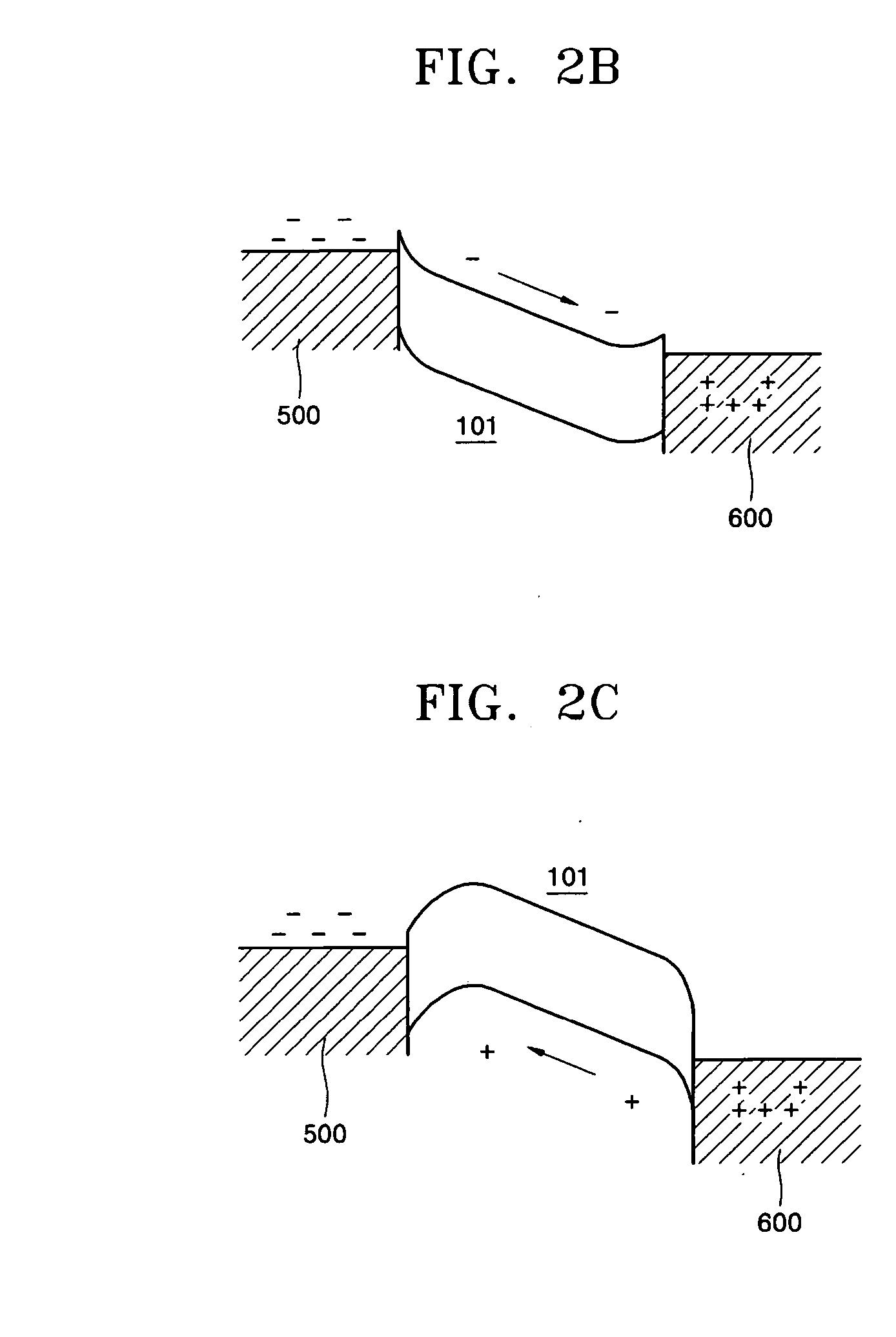
[0029] The present invention will now be described more fully with reference to the accompanying drawings, in which exemplary embodiments of the invention are shown. The invention may, however, be embodied in many different forms and should not be construed as being limited to the embodiments set forth herein; rather, these embodiments are provided so that this disclosure will be thorough and complete, and will fully convey the concept of the invention to those skilled in the art.

[0030] In the embodiments of the present invention, there is provided an SB-MOSFET that can implement an operation principle of an ambipolar transport property, which is termed by the inventor of this invention. For example, when no voltage is applied to the gate and the drain of the SB-MOSFET, no current flows through the SB-MOSFET. When positive (+) voltages are applied to the gate and the drain, electrons travel from the source to the drain, for example, in an N-type SB-MOSFET. Meanwhile, unlike the typ...


PUM


Abstract

A device using an ambipolar transport of an SB-MOSFET and a method for operating the same are provided. The SB-MOSFET includes: a silicon channel region; a source and a drain contacted on both sides of the channel region and formed of material including metal layer; and a gate formed on the channel region, with a gate dielectric layer interposed therebetween. Positive (+), 0 or negative (−) gate voltage is selectively applied to the gate, the channel becomes off-state when the gate voltage between a negative threshold voltage and a positive threshold voltage is applied, and the channel becomes a first on-state and a second on-state when the gate voltage is lower than the negative threshold voltage or higher than the positive threshold voltage. Accordingly, it is possible to implement three current states, that is, hole current, electron current, and no current. The SB-MOSFET can be applied to a multi-bit memory and / or multi-bit logic device.

Description

CROSS-REFERENCE TO RELATED PATENT APPLICATION [0001] This application claims the benefit of Korean Patent Application No. 10-2004-0109297, filed on Dec. 21, 2004, in the Korean Intellectual Property Office, the disclosure of which is incorporated herein in its entirety by reference. BACKGROUND OF THE INVENTION [0002] 1. Field of the Invention [0003] The present invention relates to a semiconductor device, and more particularly, to a device using an ambipolar transport of an Schottky Barrier Metal-Oxide-Semiconductor Field Effect Transistor (SB-MOSFET) and a method for operating the same. [0004] 2. Description of the Related Art [0005] A recent semiconductor fabrication technology makes it possible to fabricate a short-channel transistor of 100 nm or less. As the device is decreasing in size, many unexpected problems are rising. A reduction of gate length inevitably causes short channel effect. In order to fabricate transistor device with very small gate length, methods of suppressin...

Claims


Application Information

Patent Timeline
IPC IPC(8): H01L31/112
CPCG11C11/56H01L29/7839H01L29/0891
Inventor SHIN, JAE HEONJANG, MOON GYUKIM, YARK YEONLEE, SEONG JAE
Owner ELECTRONICS & TELECOMM RES INST
Why Eureka
Try Eureka