Ball grid array substrate having window and method of fabricating same

a technology of grid array substrate and substrate, which is applied in the manufacture of printed circuits, printed circuit aspects, basic electric elements, etc., can solve the problems of low heat radiation, thick packaging, and investment required to move thin core materials, and achieve the effect of reducing the thickness of packages

Inactive Publication Date: 2006-06-22
SAMSUNG ELECTRO MECHANICS CO LTD
View PDF3 Cites 35 Cited by
  • Summary
  • Abstract
  • Description
  • Claims
  • Application Information

AI Technical Summary

Problems solved by technology

The above conventional technology has a disadvantage in that the package is thick.
Furthermore, the conventional technology is problematic in that since a thin core material is employed, investment is required to move the thin core material.
The conventional technology is also problematic in that a carrier is required to handle the thin material in a package assembly process.
The above conventional technology is problematic in that heat, generated from the semiconductor chip 305, is emitted only through the wire bonds 303 but not through the insulator 301 having no thermal conductivity, thus heat radiation is low.

Method used


Image

  • Ball grid array substrate having window and method of fabricating same
  • Ball grid array substrate having window and method of fabricating same
  • Ball grid array substrate having window and method of fabricating same

Examples


Embodiment Construction

[0039] Hereinafter, a detailed description will be given of the present invention with reference to the drawings.

[0040]FIGS. 4a to 4c are sectional views of ball grid array substrates according to the present invention.

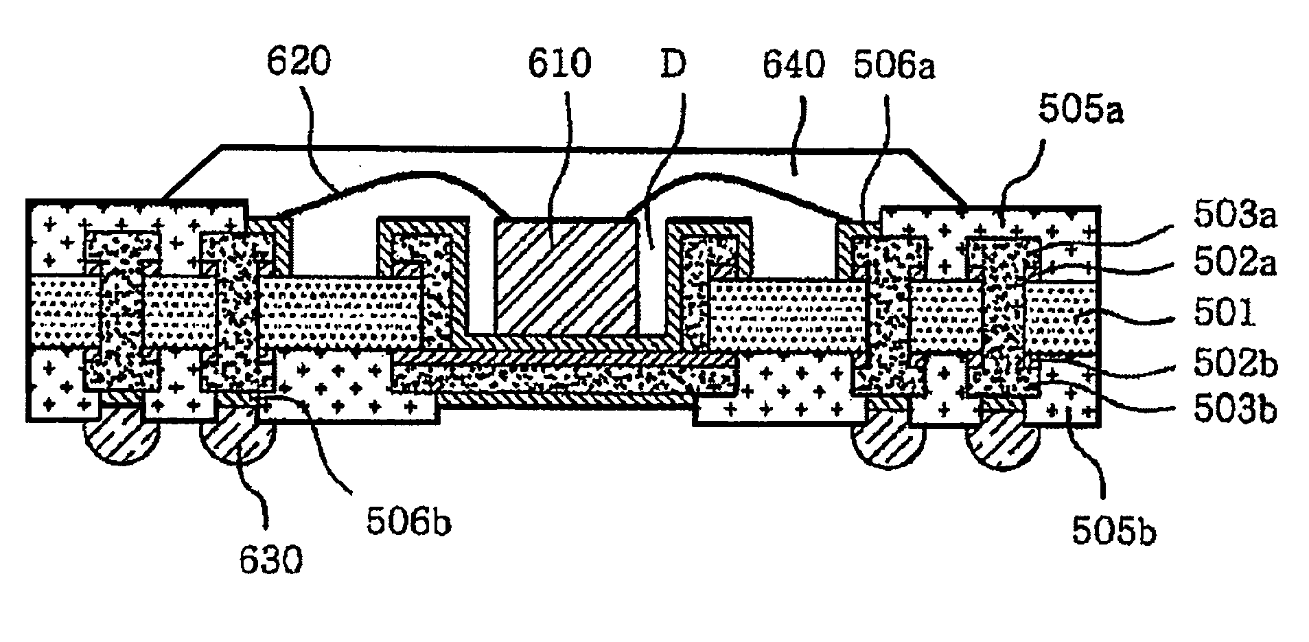
[0041] In FIG. 4a, the ball grid array substrate according to the present invention is provided with an insulating layer 501, and a via hole (E) for electrically connecting upper and lower sides of the insulating layer therethrough. Furthermore, the upper side of the insulating layer 501 includes a circuit pattern 503a and a wire bonding pad pattern, and the lower side of the insulating layer 501 includes a circuit pattern 503b and a solder ball pad pattern.

[0042] The ball grid array substrate is also provided with solder resist layers 505a, 505b, which are respectively formed on the upper and lower sides of the insulating layer 501 and which have openings at portions thereof corresponding in position to the wire bonding pad pattern and the solder ball pad pattern....


PUM


Abstract

Disclosed is a ball grid array substrate having a window formed on a core material instead of a thin core material, and wherein a semiconductor chip is mounted thereon, thereby reducing the thickness of a package, and a method of fabricating the same. The ball grid array substrate comprises a first external layer which includes first circuit patterns, wire bonding pad patterns, and a window corresponding in size to a first chip mounted therein and wherein the chip is wire-bonded to the wire bonding pad patterns. A second external layer includes second circuit patterns, a portion corresponding in position to the window of the first external layer, and solder ball pad patterns. Second chips mounted on the solder ball pad patterns. An insulating layer interposed between the first and second external layers. The window is formed through the insulating layer at a position corresponding to the window of the first external layer.

Description

INCORPORATION BY REFERENCE [0001] The present application claims priority under 35 U.S.C. §119 to Korean Patent Application No. 2004-108179 filed on Dec. 17, 2004. The content of the application is incorporated herein by reference in its entirety. BACKGROUND OF THE INVENTION [0002] 1. Field of the Invention [0003] The present invention relates, in general, to a ball grid array substrate and a method of fabricating the same and, more particularly, to a ball grid array substrate having a window, in which the window is formed on a core material instead of using a thin core material, and in which a semiconductor chip is mounted thereon, thereby reducing the thickness of a package, and a method of fabricating the same. [0004] 2. Description of the Prior Art [0005] In accordance with the recent trend toward a light, slim, short, and miniaturized package for semiconductor chips, a thickness of the package for semiconductor chips has been gradually reduced. Additionally, reduction of the th...

Claims


Application Information

Patent Timeline
Patent Type & Authority Applications(United States)
IPC IPC(8): H01L23/12
CPCH01L21/4803H01L21/4857H01L23/13H01L23/36H01L23/49816H01L2224/32145H01L2224/48091H01L2924/01046H01L2924/01078H01L2924/01079H01L2924/15153H01L2924/1517H01L2924/15311H01L2924/15331H05K1/183H05K3/064H05K3/243H05K3/403H05K3/427H05K2201/0394H05K2201/09981H05K2201/10969H05K2203/1394H01L2924/00014H01L24/48H01L2924/01019H01L2924/181H01L2924/14H01L2924/00012H01L2924/00H01L2224/45099H01L2224/45015H01L2924/207H01L23/48
Inventor LEE, JONG JIN
Owner SAMSUNG ELECTRO MECHANICS CO LTD
Why Eureka
Try Eureka