Semiconductor package and fabrication method

a technology of semiconductors and packaging, applied in the field of semiconductor packaging, can solve the problems of not solving environmental problems and not solving environmental problems, and achieve the effect of fine pitch of external connection terminals

Active Publication Date: 2006-06-22
SHINKO ELECTRIC IND CO LTD
View PDF13 Cites 30 Cited by
  • Summary
  • Abstract
  • Description
  • Claims
  • Application Information

AI Technical Summary

Benefits of technology

[0015] In view of this situation, it is an object of this invention to provide a semiconductor package and a method of fabrication thereof, which solves the environmental problem posed by the use of lead in the external connection terminals for mounting the semicond

Problems solved by technology

In view of the fact that the solder of the solder bumps normally contains lead, however, the environmental problem is not solved due to the use of lead in the solder bumps as external connection terminals or semiconductor element connection te

Method used


Image

  • Semiconductor package and fabrication method
  • Semiconductor package and fabrication method
  • Semiconductor package and fabrication method

Examples


first embodiment

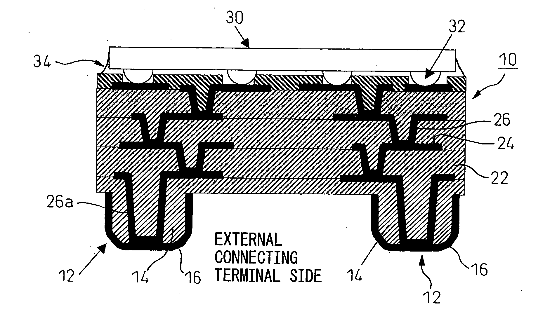
[0086]FIG. 4 is a sectional view of a semiconductor device using a semiconductor package shown in FIG. 3a. As described above, the semiconductor element connection terminal 18 is exposed from the solder resist 25 to the upper surface of the uppermost layer of the semiconductor package 10. The semiconductor element 30 having bump-like electrode terminals 32, for example, is mounted on the semiconductor package in such a manner that the electrode terminals 32 are electrically connected to the semiconductor element connection terminal 18. Further, the seal resin 34 (underfill resin) is filled in the gap between the upper surface of the semiconductor package and the semiconductor element 30. In this way, a semiconductor device is completed in which a part or the whole of the semiconductor element 30 is covered by the underfill resin. The semiconductor element 30 may be mounted on the semiconductor package by being connected to the semiconductor element connection terminal 18 by wire bo...

second embodiment

[0092] As shown in FIG. 6, the semiconductor element 30 is mounted on the upper surface of the semiconductor package 100 according to the Specifically, the semiconductor element 30 is connected to the bumps 112 formed on the upper surface of the semiconductor package 100 and filled with the insulating resin 114 while being covered with the metal layer 116. In this case, as shown in FIG. 4, the solder bumps or the like for connecting the electrodes of the semiconductor element 30 are not required. Instead, the electrodes (not shown) of the semiconductor element 30 can be directly connected to the bumps 112 projected upward from the upper surface of the semiconductor package 100 with a small amount of solder.

[0093] In mounting the semiconductor device shown in FIG. 6 on a mounting board such as the mother board or the printed wiring board, pins or solder balls (not shown) providing the external connection terminals are coupled to the lands 118, and used as a PGA (pin grid array) or a...

third embodiment

[0098]FIG. 11 is a sectional view of a semiconductor device including a semiconductor package shown in FIG. 7. During the fabrication of the semiconductor package, the semiconductor element 30 is mounted and sealed with the seal resin 34. The semiconductor element connection terminals 18 are exposed to the upper surface of the uppermost layer of the semiconductor package 10a from the solder resist 25. Thus, the semiconductor element 30 having the electrode terminals 32 in the form of bumps is mounted on the semiconductor package 10a in such a manner that the electrode terminals 32 are electrically connected to the semiconductor element connection terminals 18, and the semiconductor element 30 is covered and sealed by the epoxy seal resin 34. In this way, a semiconductor device with the whole semiconductor element 30 covered by the seal resin 34 is completed. As shown in FIG. 4, the seal resin 34 (underfill resin) can of course be covered on the gap between the semiconductor element...


PUM


Abstract

A semiconductor package and a fabrication method thereof are disclosed, whereby an environmental problem is solved by using external connection terminals or semiconductor element-mounting terminals containing a smaller amount of lead, while at the same time achieving a fine pitch of the terminals. The semiconductor package includes a board (20) including a plurality of insulating resin layers, semiconductor element-mounting terminals (18) formed on the uppermost surface of the board, and external connection terminals (12) formed on the bottom surface thereof. Each external connection terminal (12) is formed as a bump projected downward from the bottom surface of the package, and each bump is filled with the insulating resin (14) while the surface thereof is covered by a metal (16). Wiring (24), (26) including a conductor via (26a) electrically connect the metal of the metal layer 16 and the semiconductor element-mounting terminals (18).

Description

BACKGROUND OF THE INVENTION [0001] 1. Field of the Invention [0002] This invention relates to a semiconductor package and a method of fabrication thereof or, in particular, to a semiconductor package and a method of fabrication thereof in which terminals for external connection or terminals for mounting a semiconductor element are formed as bumps protruded from the package surface, each bump being filled with an insulating resin and covered with a metal. The invention further relates to a semiconductor device and a method of fabrication thereof using the semiconductor package. [0003] 2. Description of the Related Art [0004] The external connection terminals of the conventional a semiconductor package are formed of a multiplicity of balls for the ball grid array (BGA) package as shown in FIG. 1 and a multiplicity of pins for the pin grid array (PGA) package as shown in FIG. 2. [0005] Specifically, FIG. 1 shows the structure of the conventional BGA package, wherein the upper surface o...

Claims


Application Information

Patent Timeline
IPC IPC(8): H01L23/12
CPCH01L21/6835H01L23/13H01L2924/0002H01L23/49811H01L23/49822H01L2224/0401H01L2224/05568H01L2224/16H01L2924/01046H01L2924/01078H01L2924/01079H05K3/205H05K3/4007H05K3/4644H05K2201/0367H05K2201/09045H05K2201/09481H05K2203/1536H01L2224/05552H01L2224/16225H01L2924/15159
Inventor NAKAMURA, JUNICHI
Owner SHINKO ELECTRIC IND CO LTD
Why Eureka
Try Eureka