
Microelectronic package having stacked semiconductor devices and a process for its fabrication

a technology of semiconductor devices and microelectronic packages, applied in semiconductor devices, semiconductor/solid-state device details, electrical apparatus, etc., can solve problems such as topography on the surface, contact misalignment,

Active Publication Date: 2006-06-29
TESSERA INC
View PDF6 Cites 69 Cited by
  • Summary
  • Abstract
  • Description
  • Claims
  • Application Information

AI Technical Summary

Benefits of technology

[0009] The interconnect interposer element can be used to compensate for all manner of inaccuracies and errors that arise during the manufacture of the chips in the assembly. For example, the pitch of the contacts on the two chips, even if intended to be the same, can be different. Thermal gradients or the chips being made of different semiconductor materials (III-V (e.g. GaAs) vs. silicon) can stress the contacts between the two chips when the element assembly is subjected to a change in temperature, thereby causing those contacts to become misaligned. Also, the manufacturing process can cause the surface of a chip to be less than completely and perfectly planar, leading to some topography on the surface. Due to this topography, the chip contacts may not be completely coplanar. The interposer element is adaptable and can adjust to accommodate the above-identified non-uniformities and still achieve the desired interconnection between the two chips. This adjustability is achieved by using a flexible material for the interposer substrate.
[0011] It is also advantageous if the conductive posts of the interposer element terminate in solder balls. The solder balls are then used to electrically interconnect the conductive posts of the chip / interposer combination to the other chip.
[0012] In this regard, it is advantageous if the solder balls are affixed to the conductive posts or the contacts for the second chip according to the method described in commonly-assigned U.S. patent application Ser. No. 10 / 993,962, filed Nov. 19, 2004, which is entitled “Solder Ball Formation and Transfer Method,” and is hereby incorporated by reference. In this method, the solder paste, which contains a carrier and a solder, is deposited on a transfer substrate that is not substantially wettable by the solder itself; but is wettable by one of the solder paste constituents (e.g. the solder flux). Thus, the solder paste remains where it is placed on the transfer substrate because the transfer substrate is wettable by a constituent of the solder paste. Yet the solder paste is easily transferred because the transfer substrate is not wetted by the solder itself.
[0014] Once reflow is achieved, the solder masses on the transfer substrate are aligned with the conductive posts on the interposer element or the chip or the contacts on the second chip. Alignment is achieved using the methods described in the above-identified application entitled “Solder Ball Formation and Transfer Method”. Alignment is easily achieved due to the fact that the transfer substrate is made of glass and is therefore transparent.

Problems solved by technology

Thermal gradients or the chips being made of different semiconductor materials (III-V (e.g. GaAs) vs. silicon) can stress the contacts between the two chips when the element assembly is subjected to a change in temperature, thereby causing those contacts to become misaligned.
Also, the manufacturing process can cause the surface of a chip to be less than completely and perfectly planar, leading to some topography on the surface.

Method used


Image

  • Microelectronic package having stacked semiconductor devices and a process for its fabrication
  • Microelectronic package having stacked semiconductor devices and a process for its fabrication
  • Microelectronic package having stacked semiconductor devices and a process for its fabrication

Examples


Embodiment Construction

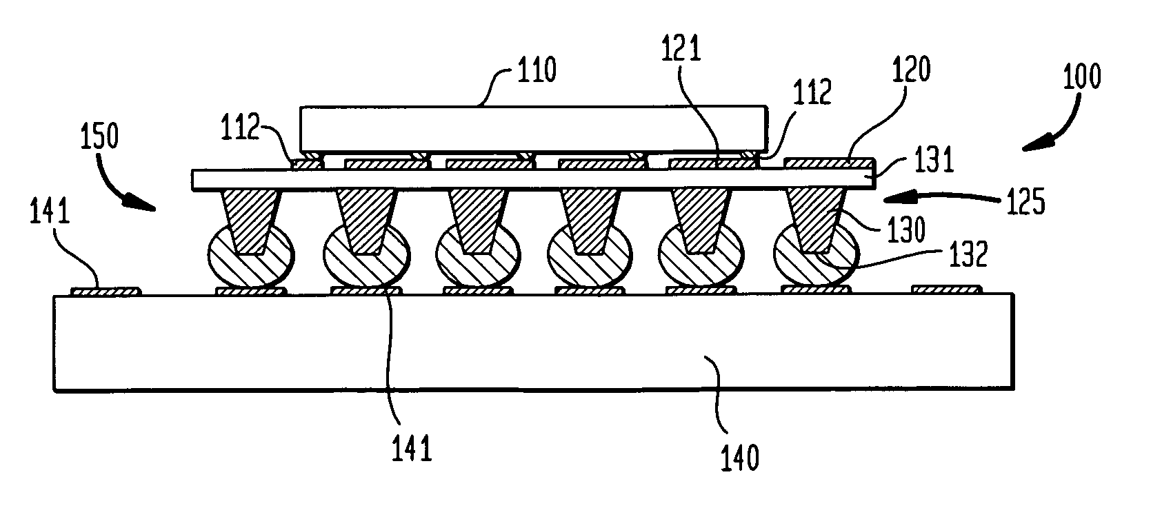
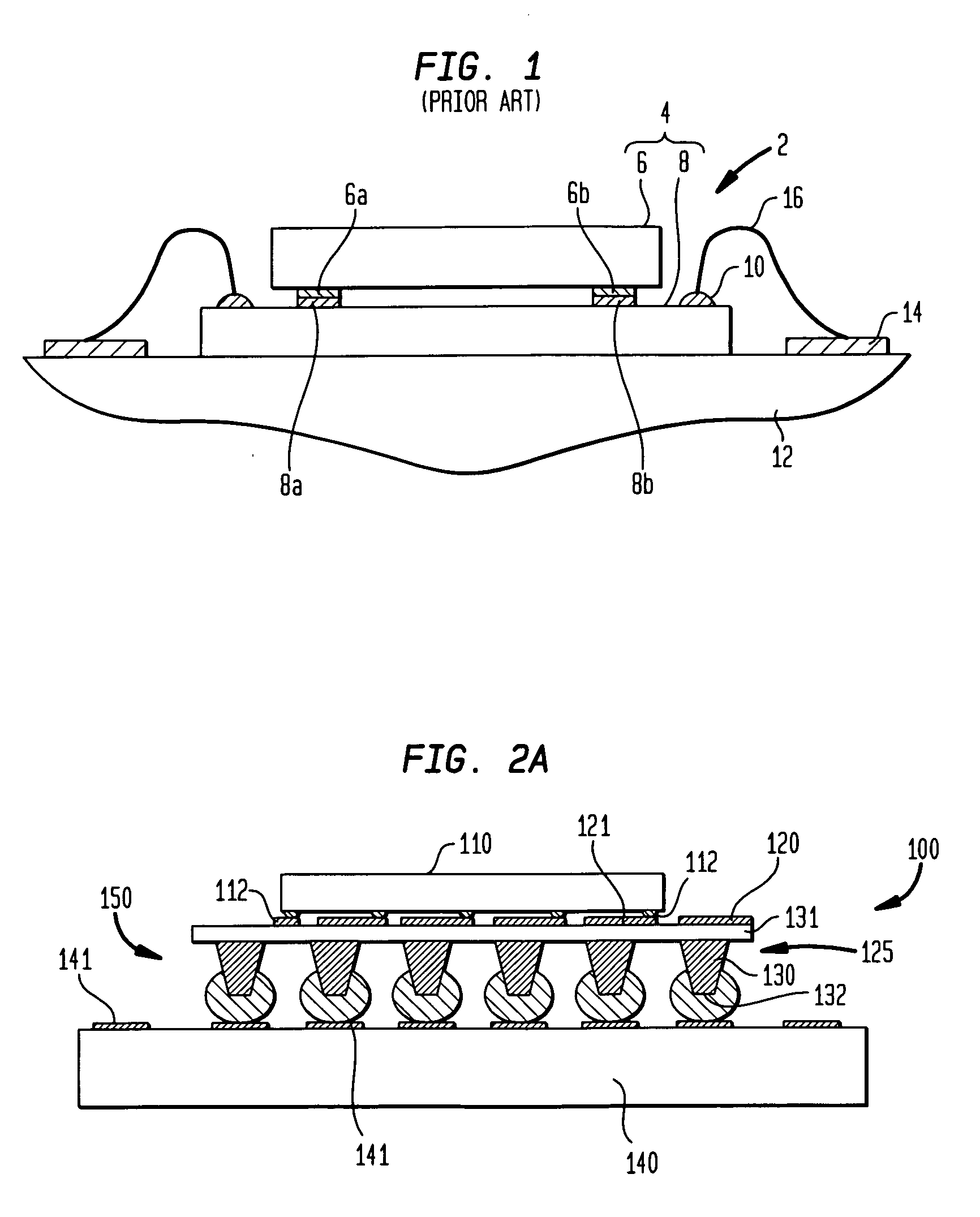
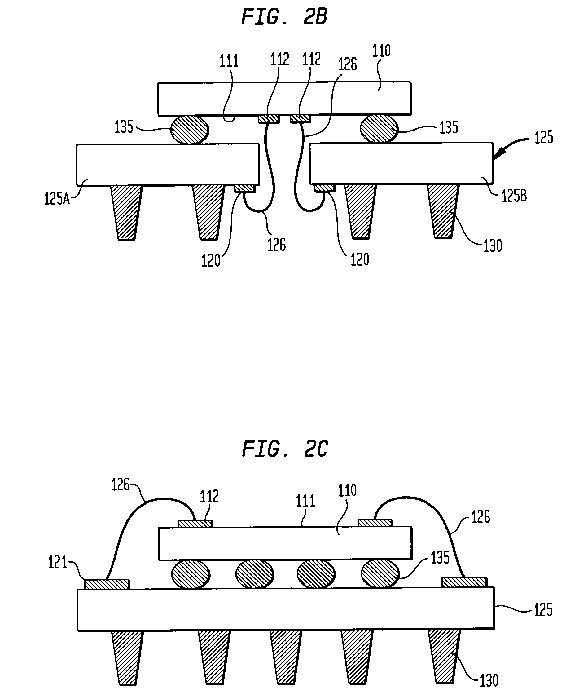
[0022] In one embodiment of the present invention a first microelectronic element is attached and electrically interconnected to a second microelectronic element. The microelectronic elements can be the same size or a different size. In the described embodiment the first microelectronic element has a smaller footprint (i.e. area) than the second microelectronic element. In one embodiment, the first microelectronic element is an assembly of a first integrated circuit device (i.e. chip) and an interposer element. This embodiment is described with reference to FIG. 2. A cross section of the packaged device 100 has a first smaller chip 110 attached to an interposer element 125. The interposer element 125 has a substrate 120 that is made of a dielectric material that, preferably, has a low modulus of elasticity, e.g., about 5 GPa or less and a large elastic range. For purposes of the present invention, a large elastic range is where the strain to failure induced by deformation (i.e. stre...


PUM


Abstract

A packaged microelectronic device having a first and second electrically interconnected microelectronic elements and a method for its manufacture. Conductive posts extend from one major surface of the first microelectronic element. The first microelectronic element is electrically interconnected to the second microelectronic element via the conductive posts. The first microelectronic element preferably has an interposer element from which the conductive posts extend. The second microelectronic element is interconnected to the interposer element via contacts on the second microelectronic element via the conductive posts. The so interconnected microelectronic elements have coordinated functionality, such as a programmable logic device wherein one microelectronic element is a field programmable gate array and the other microelectronic element is a memory device. The packaged microelectronic device is formed by using a transfer substrate to transfer solder masses onto at least some of the conductive posts extending from the first major surface of the first microelectronic element or contacts on the second microelectronic element. The solder masses are then used to electrically interconnect the conductive posts with the contacts disposed on the surface of the second microelectronic element.

Description

BACKGROUND OF THE INVENTION [0001] This invention relates to a packaged, microelectronic device having a plurality of microelectronic elements in the form of integrated circuit chips in a stacked relationship with each other. [0002] In integrated circuit devices, it is at times desired to form a packaged device that has one smaller semiconductor die or chip attached to and interconnected with another semiconductor die or chip. Such packaged devices are often referred to as stacked-chip packaged devices. Such packages are desirable and find many applications. One such application is in programmable logic devices (PLDS). For example, it is desirable to add memory to a logic chip such as a digital signal processor (DSP) chip, a central processing unit (CPU) chip or a field programmable gate array (FPGA) chip. [0003] U.S. Pat. No. 6,452,259 to Akayama describes such an LSI (large scale integration) integrated circuit device. Referring to FIG. 1, a cross-section of an LSI device is illus...

Claims


Application Information

Patent Timeline
IPC IPC(8): H01L23/34H01L23/48
CPCH01L24/73H01L25/0657H01L2924/07811H01L2924/01033H01L2924/01023H01L2924/15311H01L2924/14H01L2924/10329H01L2924/01082H01L2924/01079H01L2924/01078H01L2924/01029H01L2924/01013H01L2225/06572H01L2224/16145H01L2224/48091H01L2224/4824H01L2224/48465H01L2224/73207H01L2224/73257H01L2924/00014H01L2924/00H01L2224/05573H01L2224/05568H01L2224/0554H01L2224/05599H01L2224/0555H01L2224/0556
Inventor CRISP, RICHARD DEWITTHABA, BELGACEMHUMPSTON, GILES
Owner TESSERA INC
Features
  • Generate Ideas
  • Intellectual Property
  • Life Sciences
  • Materials
  • Tech Scout
  • Unparalleled Data Quality
  • Higher Quality Content
  • 60% Fewer Hallucinations
Learn More