Low temperature active matrix display device and method of fabricating the same

a low temperature active matrix and display device technology, applied in the direction of organic semiconductor devices, discharge tube main electrodes, incadescent cooling arrangements, etc., can solve the problems of inability to define the activated region in the tft using lithography equipment, suffer thermal deformation, etc., and achieve the effect of increasing the area of the capacitor and reducing the aperture ratio

Inactive Publication Date: 2006-06-29
ELECTRONICS & TELECOMM RES INST
View PDF7 Cites 33 Cited by
  • Summary
  • Abstract
  • Description
  • Claims
  • Application Information

AI Technical Summary

Benefits of technology

[0010] The present invention is directed to a low temperature active matrix display device and method of fabricating the same, which can solve a leakage current from a thin film transistor (TFT), the deformation of a plastic substrate, and a reduction in aperture ratio caused by an increase in the area of a capacitor.

Problems solved by technology

However, in the case of using a plastic substrate, it is impossible to define the activated region in the TFT using the lithography equipment because the plastic substrate is deformed.
If the activated region is disposed adjacent to a gate, an excessive leakage current occurs from the TFT so that the OLED cannot operate.
Also, during a low temperature activation process using a laser, the glass substrate passes the laser and avoids being deformed, whereas the plastic substrate absorbs the laser and suffers from thermal deformation.
However, in this case, a leakage current occurs between devices through a gate terminal, so that the OLED cannot operate.

Method used


Image

  • Low temperature active matrix display device and method of fabricating the same
  • Low temperature active matrix display device and method of fabricating the same
  • Low temperature active matrix display device and method of fabricating the same

Examples


Embodiment Construction

[0020] The present invention will now be described more fully hereinafter with reference to the accompanying drawings, in which exemplary embodiments of the invention are shown. It will also be understood that when a layer is referred to as being “on” another layer or substrate, it can be directly on the other layer or substrate or intervening layers may also be present. In the drawings, the thickness of layers and regions are exaggerated for clarity. The same reference numerals are used to denote the same elements throughout the specification.

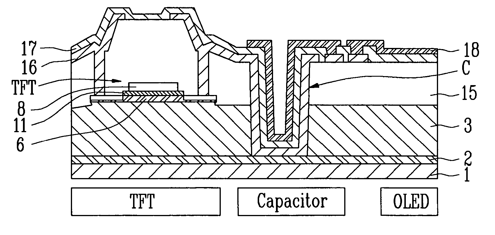
[0021]FIG. 2 is a cross-sectional view of a low temperature active matrix display device according to an exemplary embodiment of the present invention.

[0022] Referring to FIG. 2, the low temperature active matrix display device is a device that displays a unit image of a predetermined display and an organic light emitting diode (OLED) is controlled by a thin film transistor (TFT) and a capacitor C to display a predetermined image. For this f...


PUM


Abstract

Provided are a low temperature active matrix display device using a plastic substrate and method of fabricating the same. The low temperature active matrix display device includes: a plastic substrate; a reflection layer disposed on the plastic substrate; a buffer layer disposed on the reflection layer; a thin film transistor disposed on the buffer layer in a first region of the plastic substrate; an interlayer dielectric layer disposed on the thin film transistor; a capacitor disposed in a trench formed in a second region of the plastic substrate and having a first electrode connected to a source electrode and a drain electrode of the thin film transistor, the trench extending from the interlayer dielectric layer to the reflection layer; and a display device having one electrode connected to a second electrode of the capacitor. The above-described structure includes photoresist spacers to decrease a leakage current from the TFT, includes a reflector to protect the plastic substrate from deformation due to laser irradiation, and employs a three-dimensional capacitor to increase an aperture ratio.

Description

CROSS-REFERENCE TO RELATED APPLICATION [0001] This application claims priority to and the benefit of Korean Patent Application No. 2004-107026, filed Dec. 16, 2004, the disclosure of which is incorporated herein by reference in its entirety. BACKGROUND [0002] 1. Field of the Invention [0003] The present invention relates to an active matrix display device using a plastic substrate and method of fabricating the same. [0004] 2. Discussion of Related Art [0005]FIG. 1 is a cross-sectional view of a conventional active matrix display device. Referring to FIG. 1, the conventional active matrix display device is a device that displays a unit image of a predetermined display and includes a thin film transistor (TFT), a capacitor (C), and an organic light emitting diode (OLED). Here, the TFT is formed on a buffer layer 3a in a first region of a substrate 1a, and the capacitor C is formed on an interlayer dielectric layer 15a in a second region of the substrate 1a. [0006] In the above-describ...

Claims


Application Information

Patent Timeline
Patent Type & Authority Applications(United States)
IPC IPC(8): H01J61/52
CPCH01L27/3244H01L27/3262H01L27/3265H01L29/78603H01L27/1288H01L2251/5315H01L2251/5338H01L27/1255H01L29/78621H10K59/1213H10K59/1216H10K2102/3026H10K2102/311H05B33/00H05B33/10H10K59/12
Inventor KIM, YONG HAECHUNG, CHOONG HEUILEE, JIN HO
Owner ELECTRONICS & TELECOMM RES INST
Why Eureka
Try Eureka