Shift register and liquid crystal display device using the same

a technology of shift register and liquid crystal display, which is applied in the direction of digital storage, instruments, computing, etc., can solve the problems of crt having limitations in both size and weigh

Active Publication Date: 2006-06-29
LG DISPLAY CO LTD
View PDF12 Cites 44 Cited by
  • Summary
  • Abstract
  • Description
  • Claims
  • Application Information

AI Technical Summary

Problems solved by technology

However, the CRT has limitations regarding both its size and weight.

Method used


Image

  • Shift register and liquid crystal display device using the same
  • Shift register and liquid crystal display device using the same
  • Shift register and liquid crystal display device using the same

Examples


first embodiment

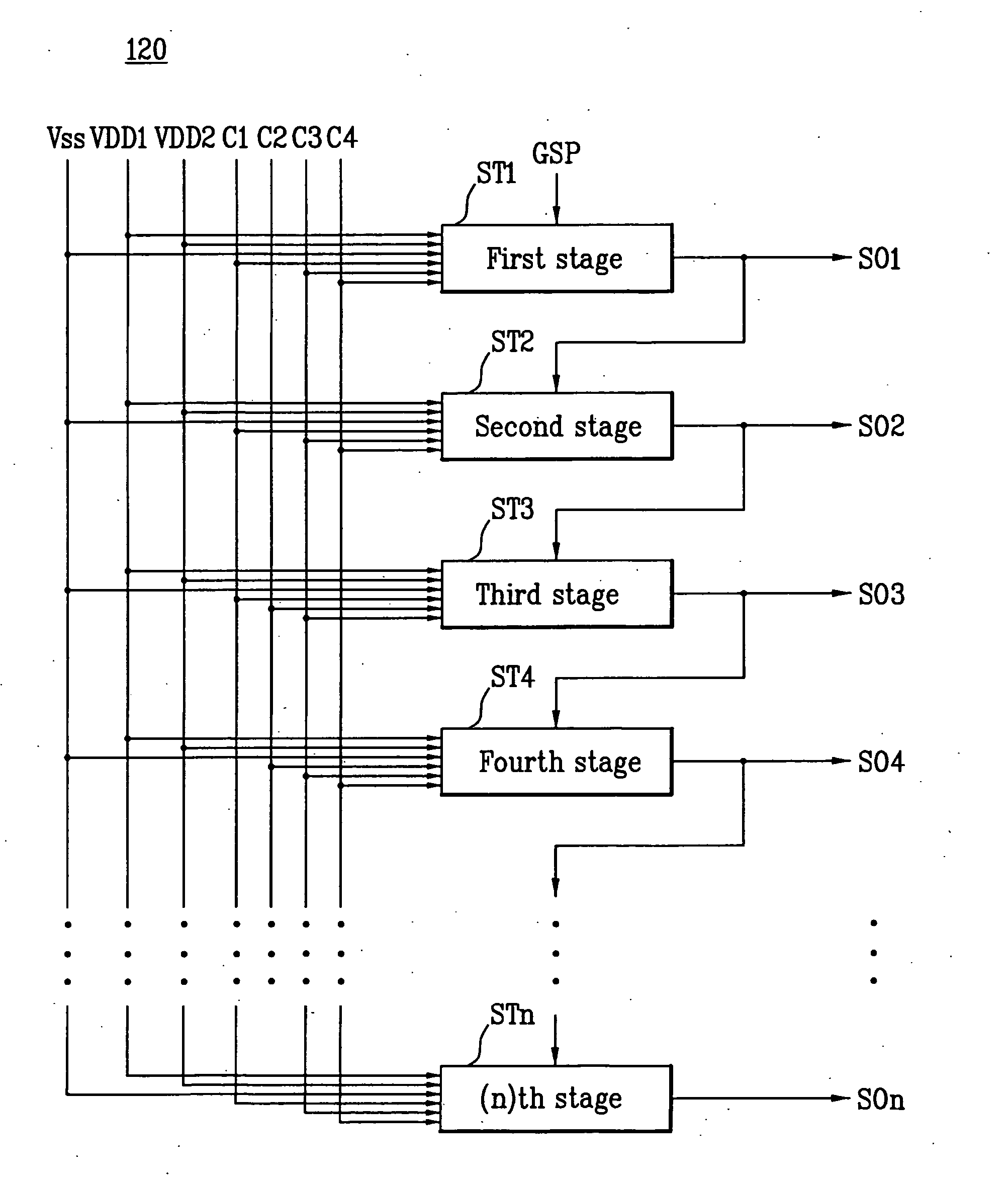
[0057]FIG. 7 is the schematic view showing the shift register 120 of the gate driver 114 shown in FIG. 5. Referring to FIG. 7, the shift register 120 according to the present invention is comprised of ‘n’ stages ST1 to STn which are connected with gate start pulse input lines, for receiving three clock signals among four clock signals C1 to C4 and the first to third supplying voltages VDD1, VDD2, and VSS outputted from the voltage generator 118.

[0058] The first stage ST1 outputs a first output signal S01 using the gate start pulse GSP and three clock signals among the four clock signals C1 to C4, such as C1, C3, and C4. Then, the second to n-th stages ST2 to STn respectively output second to n-th output signals S02 to S0n using the output signal S01 to S0(n−1) outputted from each prior stage ST1 to ST(n−1) and three clock signals among the four clock signals C1 to C4. That is, the first to n-th stages ST1 to STn sequentially output the first to n-th output signals S01 to S0n of whic...

second embodiment

[0102] After outputting the signal from each of ‘n’ stages ST1 to STn, the first to fourth clock signals C1 to C4 are in the low state by the clock mask signal Cm in some period of the blanking time which corresponds to the interval between the frames, whereby it is possible to prevent the bias stress from being applied to the respective transistors T. In the shift register and the LCD device according to the present invention, it is possible to prevent the bias stress from being applied to the transistor by the continuous logic change of the clock signals C1 to C4, and to prevent the transistor from being deteriorated.

[0103] During some sections of the blanking time, the first supplying voltage VDD1 of the high state, supplied to the shift register 220, is inversed to the low state, and the second supplying voltage VDD2 of the low state is inversed to the high state.

[0104] In the even-numbered frame, the fifth and eighth transistors T15 and T18 are maintained in the turn-on state ...


PUM


Abstract

A shift register and an LCD device to prevent the deterioration of a transistor by controlling a bias stress are disclosed. The shift register includes a plurality of stages for sequential shift signals, wherein each of the plurality of stages is connected with first and second supplying voltage input lines having opposite phases inversed by at least every frame, a start pulse input line, and at least one clock signal input line in which a phase of a first logic state is shifted in sequence, and a clock signal inputted to the clock signal input line is maintained in a second logic state different from the first logic state during a blanking time between frames.

Description

[0001] This application claims the benefit of the Korean Patent Application No. P2004-114912 filed on Dec. 29, 2004, which is hereby incorporated by reference as if fully set forth herein. BACKGROUND OF THE INVENTION [0002] 1. Field of the Invention [0003] The present invention relates to a shift register and a liquid crystal display (LCD) device using the shift register, to prevent a bias stress applied to a transistor, thereby preventing the transistor from being deteriorated. [0004] 2. Discussion of the Related Art [0005] A Cathode Ray Tube (CRT), one of flat display devices, has been widely used for monitors of a television, a measuring machine and an information terminal. However, the CRT has limitations regarding both its size and weight. Accordingly, display devices such as a liquid crystal display (LCD) device, a field emission display (FED), a plasma display panel (PDP), and a light emitting display (LED) have been actively studied, which can substitute for the CRT. [0006] ...

Claims


Application Information

Patent Timeline
Patent Type & Authority Applications(United States)
IPC IPC(8): G09G3/36
CPCG09G3/3677G09G3/3688G11C19/00G11C19/28G09G3/36
Inventor CHO, NAM WOOK
Owner LG DISPLAY CO LTD
Why Eureka
Try Eureka