Liquid crystal display device and fabricating method thereof

a technology of liquid crystal display and fabrication method, which is applied in the direction of optics, instruments, electrical equipment, etc., can solve the problems of complicated fabrication process and increase the manufacturing cost of the liquid crystal display panel, and achieve the effect of simplifying the process

Inactive Publication Date: 2006-06-29
LG DISPLAY CO LTD
View PDF15 Cites 40 Cited by
  • Summary
  • Abstract
  • Description
  • Claims
  • Application Information

AI Technical Summary

Benefits of technology

[0018] An advantage of the present invention is to provide a thin film transistor substrate of horizontal electric field applying type and fabricating method thereof that are adaptive for simplifying a process.
[0019] Additional features and advantages of the invention will be set forth in the description which follows, and in part will be apparent from the description, or may be learned by practice of the invention. The advantages of the invention will be realized and attained by the structure particularly pointed out in the written description and claims hereof as well as the appended drawings.
[0020] To achieve these and other advantages and in accordance with the purpose of the present invention, as embodied and broadly described, a liquid crystal display device comprising a gate line on a substrate; a data line crossing the gate line with a gate insulating film therebetween, wherein the data and gate lines define a pixel area; a thin film transistor including a gate electrode connected to the gate line, a source electrode connected to the data line, a drain electrode opposed to the source electrode and a semiconductor pattern defining a channel between the source electrode and the drain electrode; a common line on the substrate and substantially parallel to the gate line; a common electrode extended from the common line into the pixel area; and a pixel electrode extended from the drain electrode into the pixel area to form a horizontal electric field with the common electrode, wherein the gate line and the common line have a first conductive layer group having at least double conductive layers, and the common electrod

Problems solved by technology

In particular, because the thin film transistor substrate includes the semiconductor process and requires the plurality of mask processes, it has a complicated fabricating process which is a major factor in increased manufacturing costs of the liq

Method used


Image

  • Liquid crystal display device and fabricating method thereof
  • Liquid crystal display device and fabricating method thereof
  • Liquid crystal display device and fabricating method thereof

Examples


Embodiment Construction

[0038] Reference will now be made in detail to embodiments of the present invention, examples of which are illustrated in the accompanying drawings.

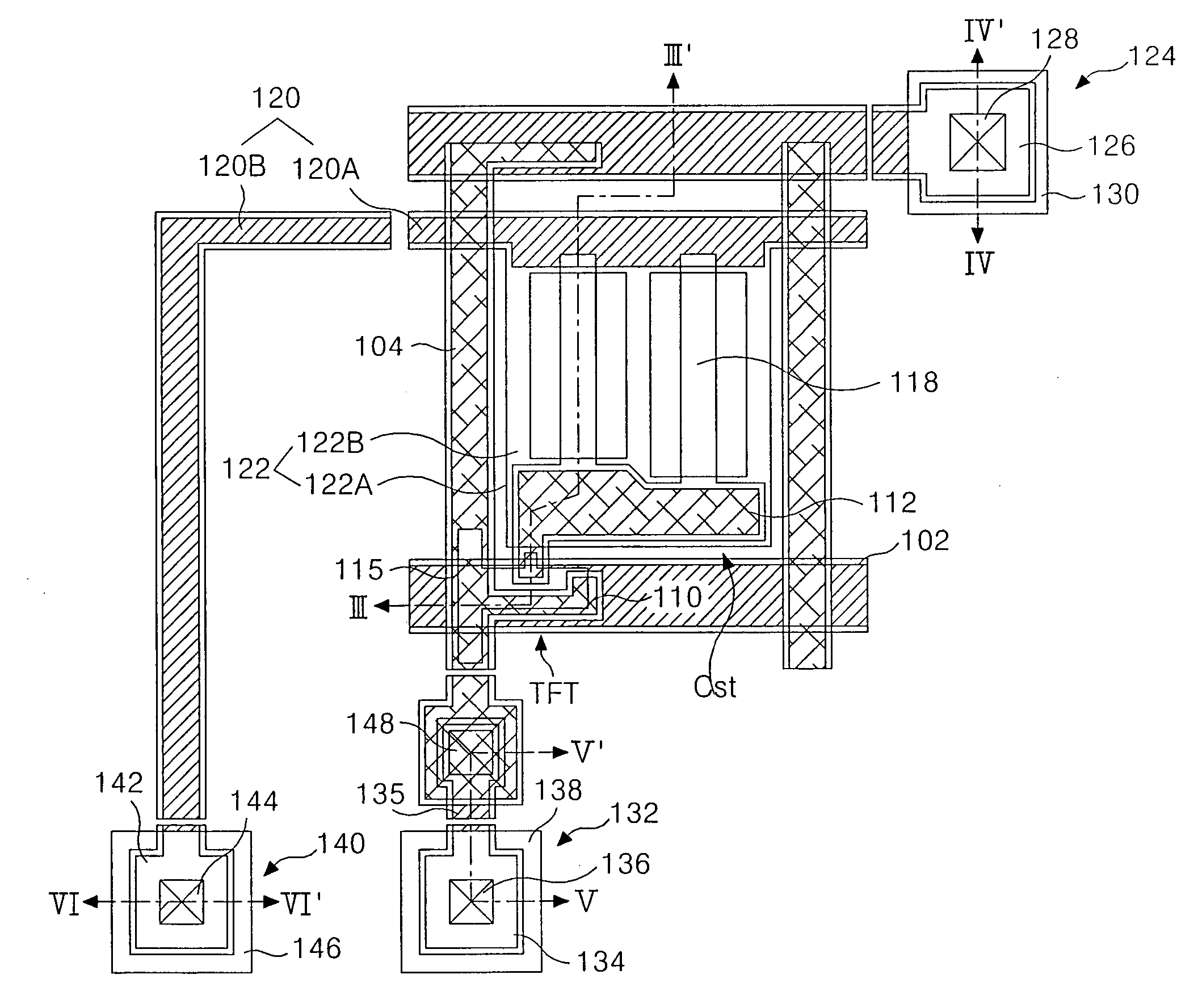
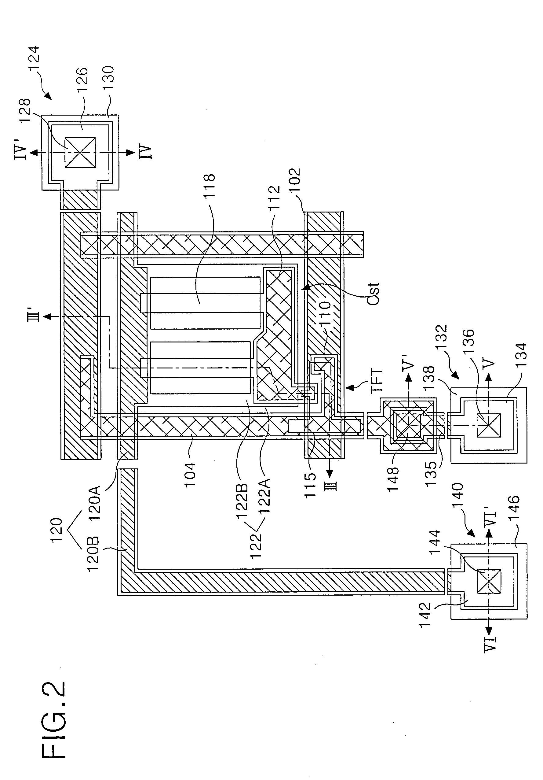
[0039]FIG. 2 is a plan view illustrating a structure of a thin film transistor substrate of a horizontal electric field applying type according to an embodiment of the present invention, and FIG. 3 are section views of the thin film transistor substrate taken along the III-III′, IV-IV′, V-V′, and VI-VI′ lines in FIG. 2.

[0040] In FIG. 2 and FIG. 3, the thin film transistor substrate of a horizontal electric field applying type includes a gate line 102 and a data line 104 provided on a lower substrate 150 in such a manner to cross each other with a gate insulating film 152 therebetween and defining a pixel area, a thin film transistor TFT connected to the gate line 102, the data line 104, and a pixel electrode 118. The pixel electrode 118 and a common electrode 122 form a horizontal electric field at said pixel area. A common line 120 is...


PUM


Abstract

A LCD device includes a gate line on a substrate and a data line crossing the gate line to define a pixel area; a thin film transistor source and drain electrodes; a common line parallel to the gate line; a common electrode extended from the common line and a pixel electrode extending from the drain electrode wherein the gate line and the common line have a first conductive layer group having at least double conductive layers, and the common electrode is formed by an extension of at least one transparent conductive layer of the common line; and the gate line, the source electrode and the drain electrode have a second conductive layer group having at least double conductive layers, and the pixel electrode is formed by an extension of at least one transparent conductive layer of the drain electrode.

Description

[0001] This application claims the benefit of Korean Patent Application No. P2004-112578 filed in Korea on Dec. 24, 2004, which is hereby incorporated by reference for all purposes as if fully set forth herein. BACKGROUND OF THE INVENTION [0002] 1. Field of the Invention [0003] This invention relates to a liquid crystal display device using a horizontal electric field, and more particularly to a thin film transistor substrate of horizontal electric field applying type and a fabricating method thereof that are adaptive for simplifying a process. [0004] 2. Discussion of the Related Art [0005] Generally, a liquid crystal display (LCD) controls light transmittance of a liquid crystal having a dielectric anisotropy using an electric field to thereby display a picture. To this end, the LCD includes a liquid crystal display panel for displaying a picture by a liquid crystal cell matrix, and a driving circuit for driving the liquid crystal display panel. [0006] In FIG. 1, a related art liqu...

Claims


Application Information

Patent Timeline
IPC IPC(8): G02F1/1343
CPCG02F1/134363G02F2001/136231G02F2001/13629G02F1/136231G02F1/13629G02F1/136
Inventor AHN, BYUNG CHUL
Owner LG DISPLAY CO LTD
Why Eureka
Try Eureka