
Method of cleaning silicon nitride layer

Inactive Publication Date: 2006-06-29
DONGBU ELECTRONICS CO LTD
View PDF3 Cites 4 Cited by
  • Summary
  • Abstract
  • Description
  • Claims
  • Application Information

AI Technical Summary

Benefits of technology

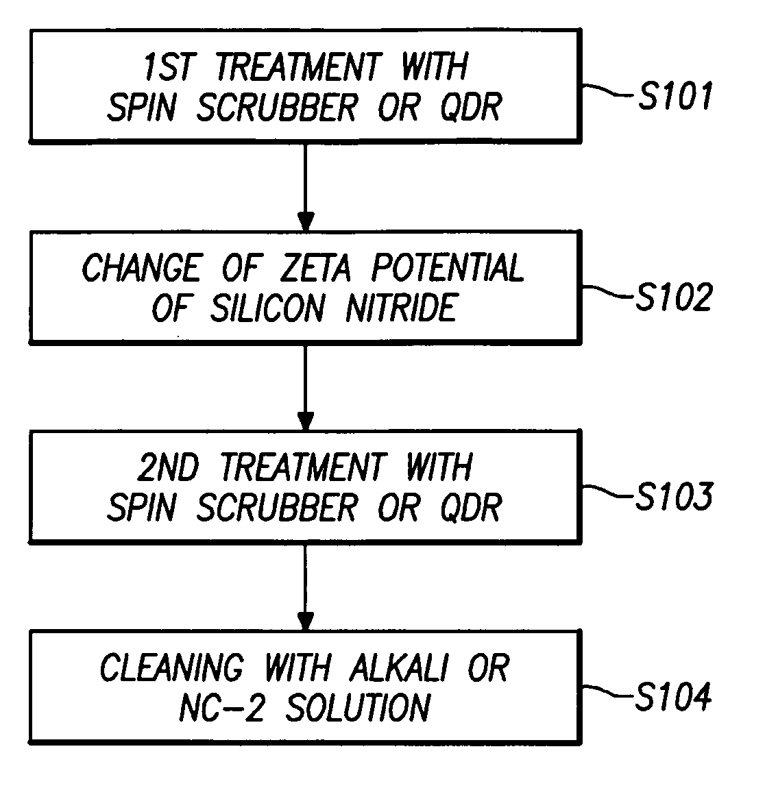
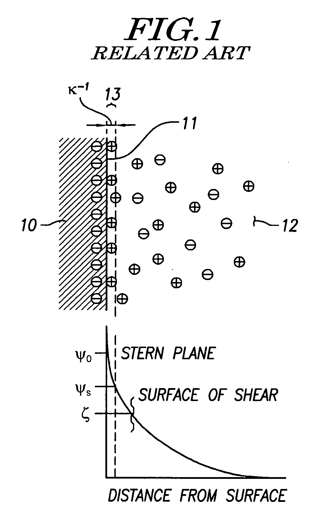
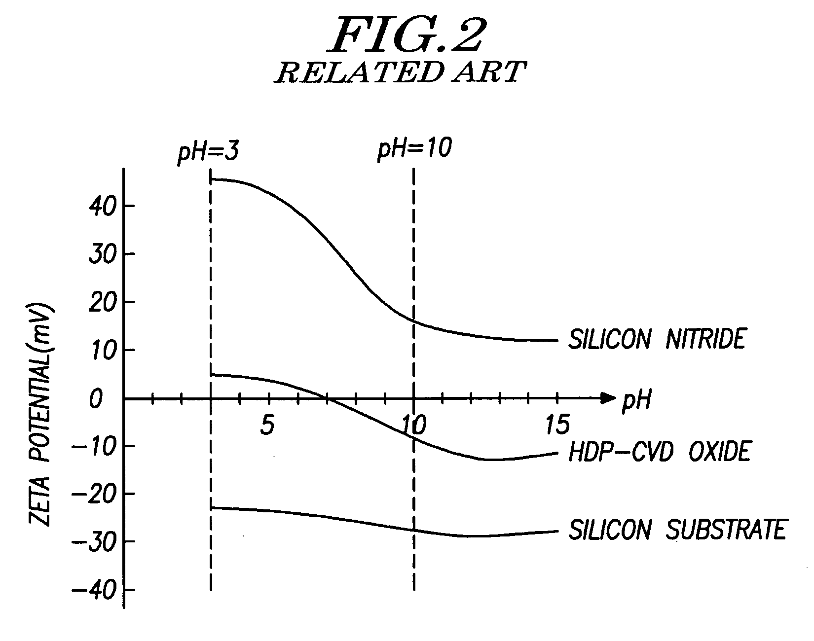
[0014] Exemplary, non-limiting embodiments of the present invention provide a method of cleaning a silicon nitride layer on a substrate so as to effectively remove negatively-charged impurities such as polymers and particles from the silicon nitride layer by changing the zeta potential of the silicon nitride layer from positive to negative.
[0017] In the method, the changing of the zeta potential can include dipping the substrate into a second solution selected from the group consisting of an SC-1 solution, an NC-2 solution, and an alkali solution. In this case, the second solution can further have surfactant. The alkali solution can be an ammonium hydroxide solution or a tri-methyl ammonium hydroxide solution and can maintain the normal temperature.

Problems solved by technology

So, although a cleaning process is performed, such impurities can be hardly removed from the silicon nitride layer.
However, these techniques are separately employed in general and do not use electrochemical surface properties of the silicon nitride layer.
So these conventional techniques may fail to provide effective cleaning for the silicon nitride layer.

Method used


Image

  • Method of cleaning silicon nitride layer
  • Method of cleaning silicon nitride layer
  • Method of cleaning silicon nitride layer

Examples


Embodiment Construction

[0024] An exemplary, non-limiting embodiment of the present invention will now be described more fully hereinafter with reference to the accompanying drawings. This invention may, however, be embodied in many different forms and should not be construed as limited to the exemplary embodiment set forth herein. Rather, the disclosed embodiment is provided so that this disclosure will be thorough and complete, and will fully convey the scope of the invention to those skilled in the art. The principles and features of this invention may be employed in varied and numerous embodiments without departing from the scope of the invention.

[0025] In is noted that well-known structures and processes are not described or illustrated in detail to avoid obscuring the essence of the present invention. It is also noted that the figures are not drawn to scale.

[0026]FIG. 3 is a flow chart showing a cleaning method of a silicon nitride layer in accordance with an exemplary embodiment of the present inv...


PUM


Abstract

A method of cleaning a silicon nitride layer on a substrate is provided to effectively remove negative-charged impurities such as polymer and particle from the silicon nitride layer. In the method, the zeta potential of the silicon nitride layer is changed from positive to negative, and then the silicon nitride layer is cleaned with a first solution selected from an alkali solution and an NC-2 solution. So the negatively-charged impurities can be easily removed due to a repulsion force. The substrate can be treated with spin scrubber or quick dump rinse before and / or after the changing of the zeta potential. To change the zeta potential, the substrate can be dipped into a second solution such as an SC-1 solution, an NC-2 solution, and an alkali solution.

Description

[0001] This U.S. non-provisional application claims priority under 35 U.S.C. §119 from Korean Patent Application No. 2004-115806, which was filed in the Korean Intellectual Property Office on Dec. 29, 2004, the contents of which are incorporated by reference herein in its entirety. BACKGROUND OF THE INVENTION [0002] 1. Field of the Invention [0003] The present invention relates generally to a wafer cleaning technique in semiconductor fabrication and, more particularly, to a method of cleaning a silicon nitride layer so as to effectively remove impurities such as polymer and particle from the silicon nitride layer. [0004] 2. Description of the Related Art [0005] As is well known in the art, a silicon nitride layer has a denser and tighter structure in comparison with a silicon oxide layer, so the silicon nitride layer has excellent ability to prevent infiltration of moisture or alkali ions, and thus is typically used as a passivation layer. Furthermore, the silicon nitride layer is n...

Claims


Application Information

Patent Timeline
IPC IPC(8): H01L21/302
CPCH01L21/0206Y10S438/906H01L21/302H01L21/304
Inventor KWON, DAE HEOK
Owner DONGBU ELECTRONICS CO LTD
Learn More