Non-volatile memory device and manufacturing method and operating method thereof

Active Publication Date: 2006-07-06
POWERCHIP SEMICON MFG CORP
View PDF7 Cites 9 Cited by
  • Summary
  • Abstract
  • Description
  • Claims
  • Application Information

AI Technical Summary

Benefits of technology

[0009] Accordingly, the present invention provides a non-volatile memory device and a fabrication method and an operating method thereof

Problems solved by technology

Thus, an abnormal punch through between the source region and the drain region easily occurs, which greatly affect the electrical performance of the memory cell.
Moreover, two neighboring memory cells may interfere with each other to slow down the operating speed of the

Method used


Image

  • Non-volatile memory device and manufacturing method and operating method thereof
  • Non-volatile memory device and manufacturing method and operating method thereof
  • Non-volatile memory device and manufacturing method and operating method thereof

Examples


Example

[0041] Reference will now be made in detail to the present preferred embodiments of the invention, examples of which are illustrated in the accompanying drawings. Wherever possible, the same reference numbers are used in the drawings and the description to refer to the same or like parts.

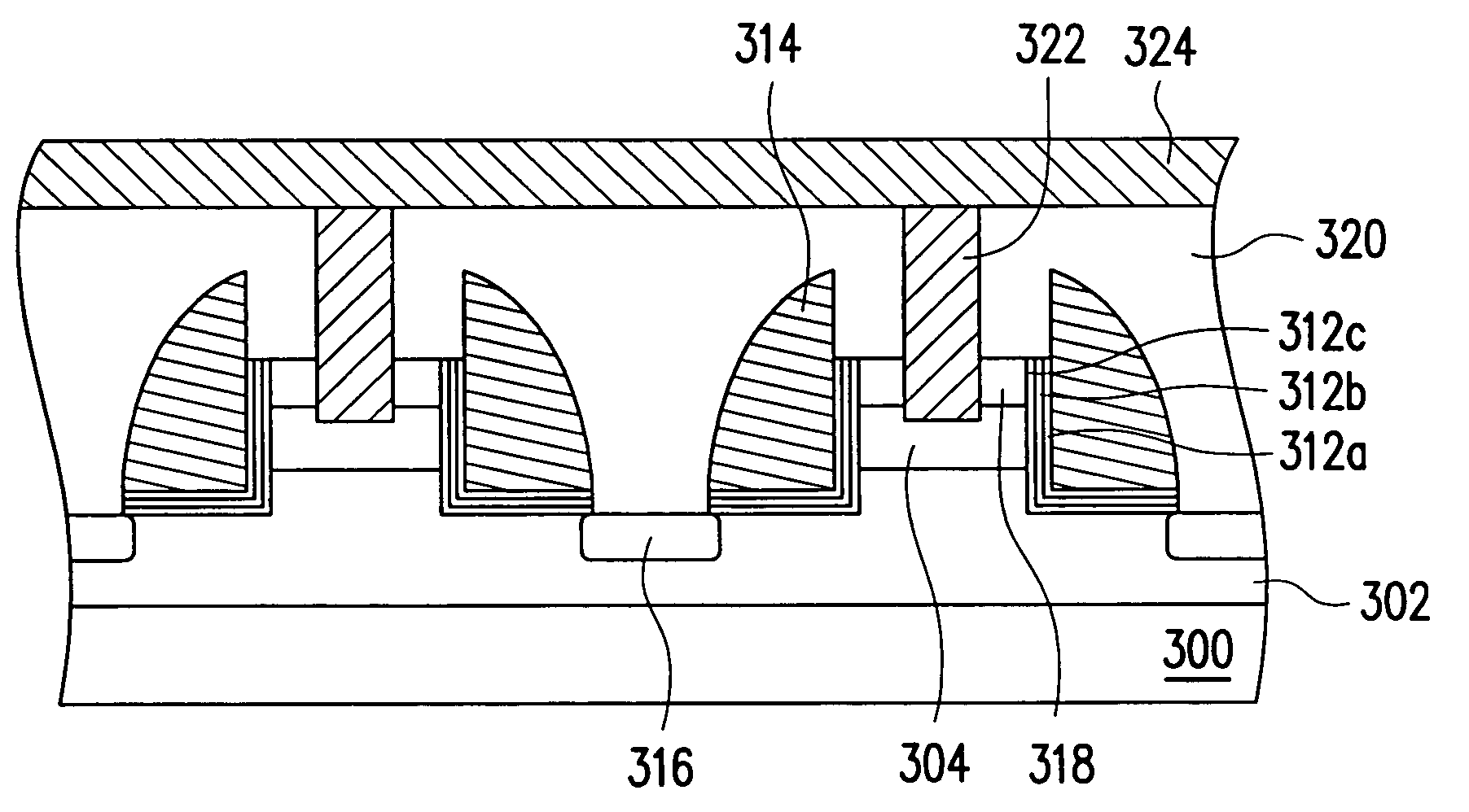
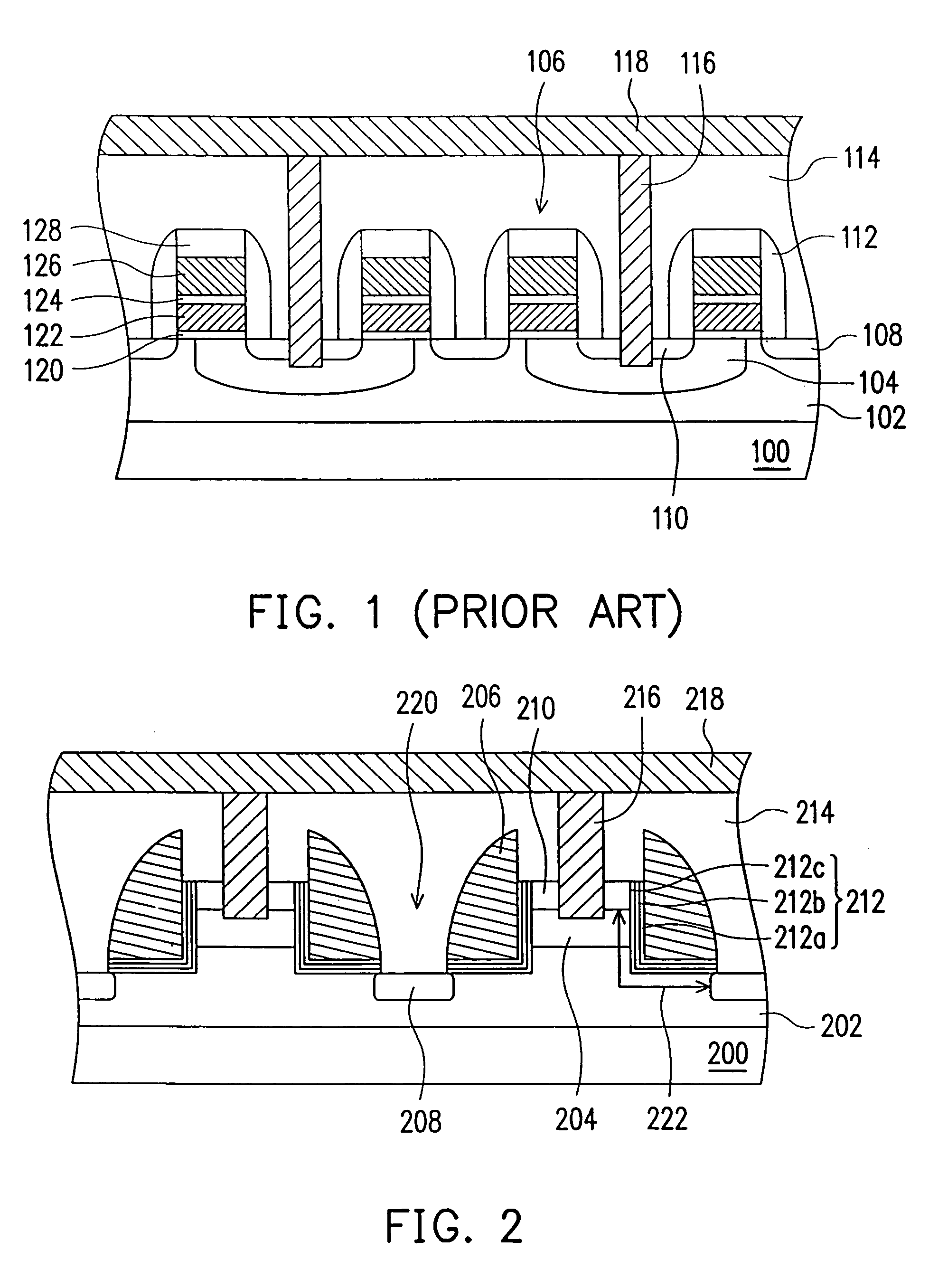
[0042]FIG. 2 is a schematic, cross-sectional view of a non-volatile memory device structure. The following discussion will be based on a bi-directional tunneling program / erase NOR (BiNOR) array of non-volatile memory for illustration.

[0043] Referring to FIG. 2, the non-volatile memory device of the present invention is formed with a p-type substrate 200, a deep n-type well region 202, a p-type well region 204, a control gate 206, a source region 208, a drain region 210, a composite dielectric layer 212, an interlayer dielectric layer 214, a conductive plug 216, a conductive line 218 (bit line).

[0044] The p-type substrate 200 includes a plurality of parallel arranged trenches 220. The deep n-type ...


PUM


Abstract

A non-volatile memory device having a substrate, an n type well, a p type well, a control gate, a composite dielectric layer, a source region and a drain region is provided. A trench is formed in the substrate. The n type well is formed in the substrate. The p type well is formed in the substrate above the n type well. The junction of p type well and the n type well is higher than the bottom of the trench. The control gate which protruding the surface of substrate is formed on the sidewalls of the trench. The composite dielectric layer is formed between the control gate and the substrate. The composite dielectric layer includes a charge-trapping layer. The source region and the drain region are formed in the substrate of the bottom of the trench respectively next to the sides of the control gate.

Description

CROSS-REFERENCE TO RELATED APPLICATION [0001] This application claims the priority benefit of Taiwan application serial no. 94100019, filed on Jan. 3, 2005. All disclosure of the Taiwan application is incorporated herein by reference. BACKGROUND OF THE INVENTION [0002] 1. Field of the Invention [0003] The present invention relates to a semiconductor device. More particularly, the present invention relates to a non-volatile memory (NVM) device and a manufacturing method and an operating method thereof. [0004] 2. Description of Related Art [0005] Electrically erasable programmable read only memory (EEPROM) is a type of non-volatile memory that allows multiple data reading, writing and erasing operations. In addition, the stored data will be retained even after power to the device is removed. With these advantages, it has been broadly applied in personal computer and electronic equipment. [0006] A typical flash memory device has a floating gate and a control gate fabricated using doped...

Claims


Application Information

Patent Timeline
IPC IPC(8): H01L21/8242H01L21/28H01L21/336H01L21/8246H01L21/8247H01L27/115H01L29/792
CPCH01L21/28282H01L27/115H01L27/11568H01L29/66833H01L29/792H01L29/7926Y10S438/954H01L29/40117H10B69/00H10B43/30
Inventor WONG, WEI-ZHEYANG, CHING-SUNGCHO, CHIH-CHEN
Owner POWERCHIP SEMICON MFG CORP
Why Eureka
Try Eureka