Liquid crystal display device

a liquid crystal display and display device technology, applied in static indicating devices, non-linear optics, instruments, etc., can solve the problems of deteriorating the picture quality of the lcd device, substantially impossible methods, and reducing the effective time, so as to prevent an inferiority, effectively prevent an inferiority, and reduce the size of the lcd.

Active Publication Date: 2006-07-06
LG DISPLAY CO LTD
View PDF6 Cites 31 Cited by
  • Summary
  • Abstract
  • Description
  • Claims
  • Application Information

AI Technical Summary

Benefits of technology

[0017] A disclosed LCD device prevents an inferiority thereof due to a signal lowering by increasing a pulse width of a scan signal applied to a thin film transistor inside a pixel region through a gate line more than the turned on time of the thin film transistor. Also described is an LCD device that effectively prevents an inferiority thereof due to a signal lowering by applying a scan signal overlapped to an adjacent gate line without increasing the LCD size or the fabrication cost.

Problems solved by technology

The rectangular wave decreases the turned ON time of the thin film transistor, thereby decreasing an effective time that an image signal is charged to the liquid crystal panel and thus deteriorating a picture quality of the LCD device.
However, since a region for forming a gate driving unit is greatly increased, the method was substantially impossible.

Method used


Image

  • Liquid crystal display device
  • Liquid crystal display device
  • Liquid crystal display device

Examples


Embodiment Construction

[0032] Reference will now be made in detail to the preferred embodiments of the present invention, examples of which are illustrated in the accompanying drawings.

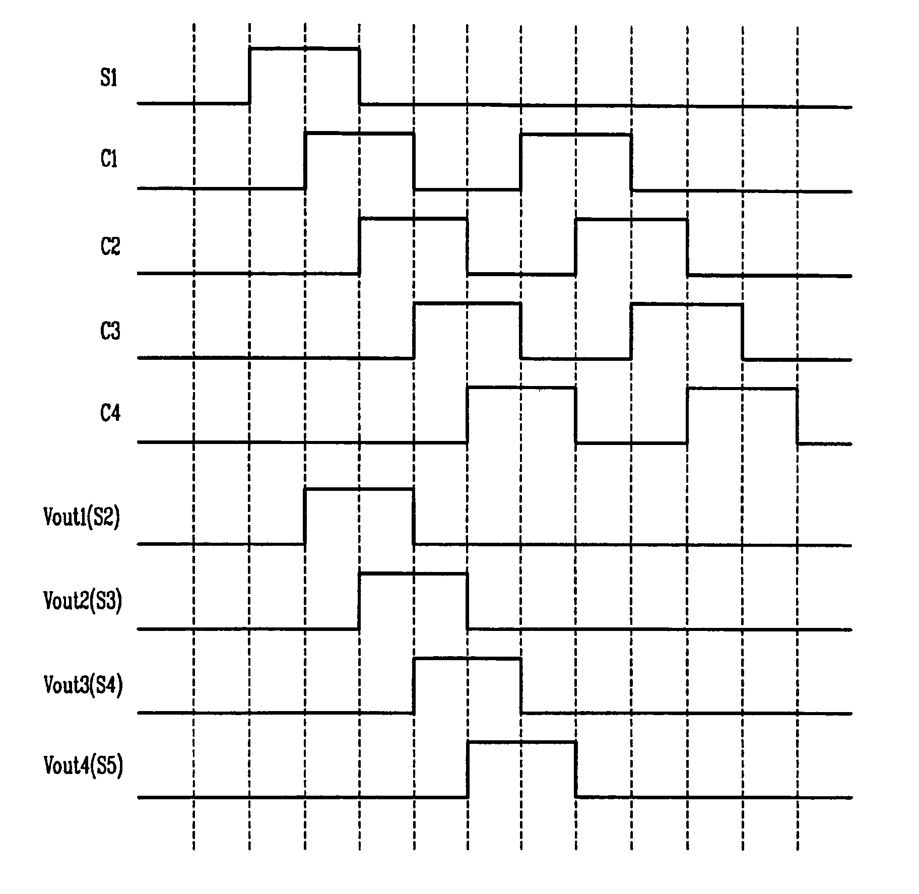
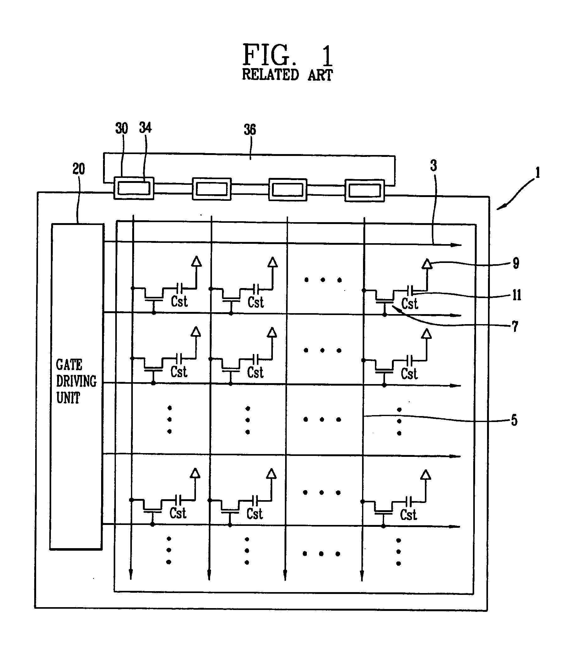
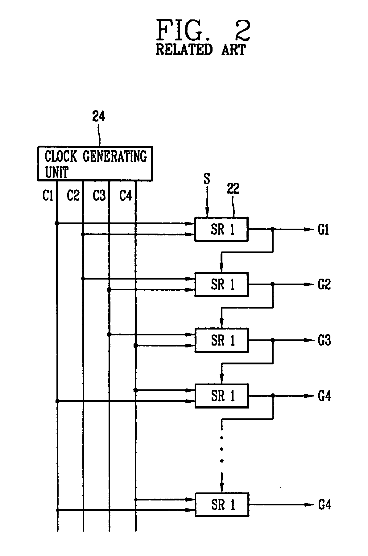
[0033] In order to prevent a distortion of a scan signal applied to a thin film transistor formed at a pixel region (that is, a tail of an output waveform due to a signal lowering), the following methods are used. First, a size of the thin film transistor is increased thereby to minimize an influence by a lower field effect mobility. Second, the thin film transistor is formed of poly-crystalline silicon not amorphous silicon thereby to increase a field effect mobility. The first method is substantially impossible because the size of a gate driving unit integrally formed at a liquid crystal panel is increased as the size of the thin film transistor is increased. The second method is substantially possible but is not effective due to a high fabrication cost and complicated fabrication processes.

[0034] The present invention ...


PUM


Abstract

A liquid crystal display (LCD) device comprises a liquid crystal panel having a plurality of pixel regions defined by a plurality of gate lines and data lines, each pixel region associated with a thin film transistor, a gate driving unit having an amorphous semiconductor and integrally formed with the liquid crystal panel capable of sending a scan signal to the gate lines having a pulse width longer than a turned on time of the thin film transistor located within the pixel region, and a data driving unit connected to the data lines capable of sending an image signal to the data lines.

Description

[0001] This application claims the benefit of Korean Patent Application No. 10-2004-0118456, filed on Dec. 31, 2004, which is hereby incorporated by reference as if fully set forth herein. BACKGROUND OF THE INVENTION [0002] 1. Field of the Invention [0003] The present invention relates to a liquid crystal display (LCD) device, and more particularly, to a LCD device capable of preventing an inferiority thereof due to a signal lowering by increasing a set pulse width of a scan signal applied to a gate line. [0004] 2. Description of the Related Art [0005] A liquid crystal display (LCD) device is a transparent flat panel display device, and is being widely applied to each kind of electronic device such as a mobile phone, a PDA, a notebook computer, etc. Since the LCD device has light, thin, short and small characteristics and can implement a high picture quality, it is being used more than other flat panel display devices. Moreover, as a demand for a digital TV, a high picture quality T...

Claims


Application Information

Patent Timeline
Patent Type & Authority Applications(United States)
IPC IPC(8): G09G3/36
CPCG09G3/3677G09G2300/0417G09G2310/0205G09G2310/0251G09G2310/08G02F1/133
Inventor JANG, YONG-HOKIM, BINNMOON, SU-HWANCHO, NAM-WOOKYOON, SOO-YOUNG
Owner LG DISPLAY CO LTD
Why Eureka
Try Eureka