Method of planarizing an inter-metal insulation film

a technology of inter-metal insulation and planarization, which is applied in the direction of semiconductor/solid-state device manufacturing, basic electric elements, electric apparatus, etc., can solve the problems of difficult to obtain a completely planarized upper surface of the resulting structure, insufficient cmp process to remove a significant quantity of insulating material, and insufficient planarization to an undesirable depth. , to achieve the effect of improving process throughput, excellent planarization characteristics and good control thickness

Active Publication Date: 2006-07-06
SAMSUNG ELECTRONICS CO LTD
View PDF5 Cites 2 Cited by
  • Summary
  • Abstract
  • Description
  • Claims
  • Application Information

AI Technical Summary

Benefits of technology

[0016] Embodiments of the invention provide a method of forming a planarized inter-metal insulation film adapted for use in semiconductor device having better controlled thickness and excellent planarization characteristics with improved process throughput.

Problems solved by technology

However, even in processes using these beneficial materials, it is difficult to obtain a completely planarized upper surface of the resulting structure.
Unfortunately, this additional thermal treatment process usually requires the application of high-temperatures which cause collateral problems, such as the short channel effect in active devices formed within the semiconductor device.
In certain circumstances, the removal of this upper portion of the stepped inter-metal insulation film may result in planarization to an undesirable depth.
Additionally, a CMP process sufficient to remove the significant quantity of insulating material is often overly time consuming.
Further, the irregular upper surface of the inter-metal insulation layer to which the CMP process is applied makes it difficult to precisely align and remove a specific thickness of material forming the insulation film.
Thus, the CMP process may result in a non-uniform upper surface that varies with semiconductor wafer positioning under the CMP process.
Excellent planarization characteristics, therefore, cannot be obtained using the conventional methods.

Method used


Image

  • Method of planarizing an inter-metal insulation film
  • Method of planarizing an inter-metal insulation film
  • Method of planarizing an inter-metal insulation film

Examples


Embodiment Construction

[0024] Embodiments of the invention will now be described in some additional detail with reference to the accompanying drawings. However, many other embodiments, as well as modifications and alterations to the illustrated embodiments, are possible beyond the teaching examples presented here. Thus, the scope of the invention should not be construed as being limited to only the exemplary embodiments set forth herein.

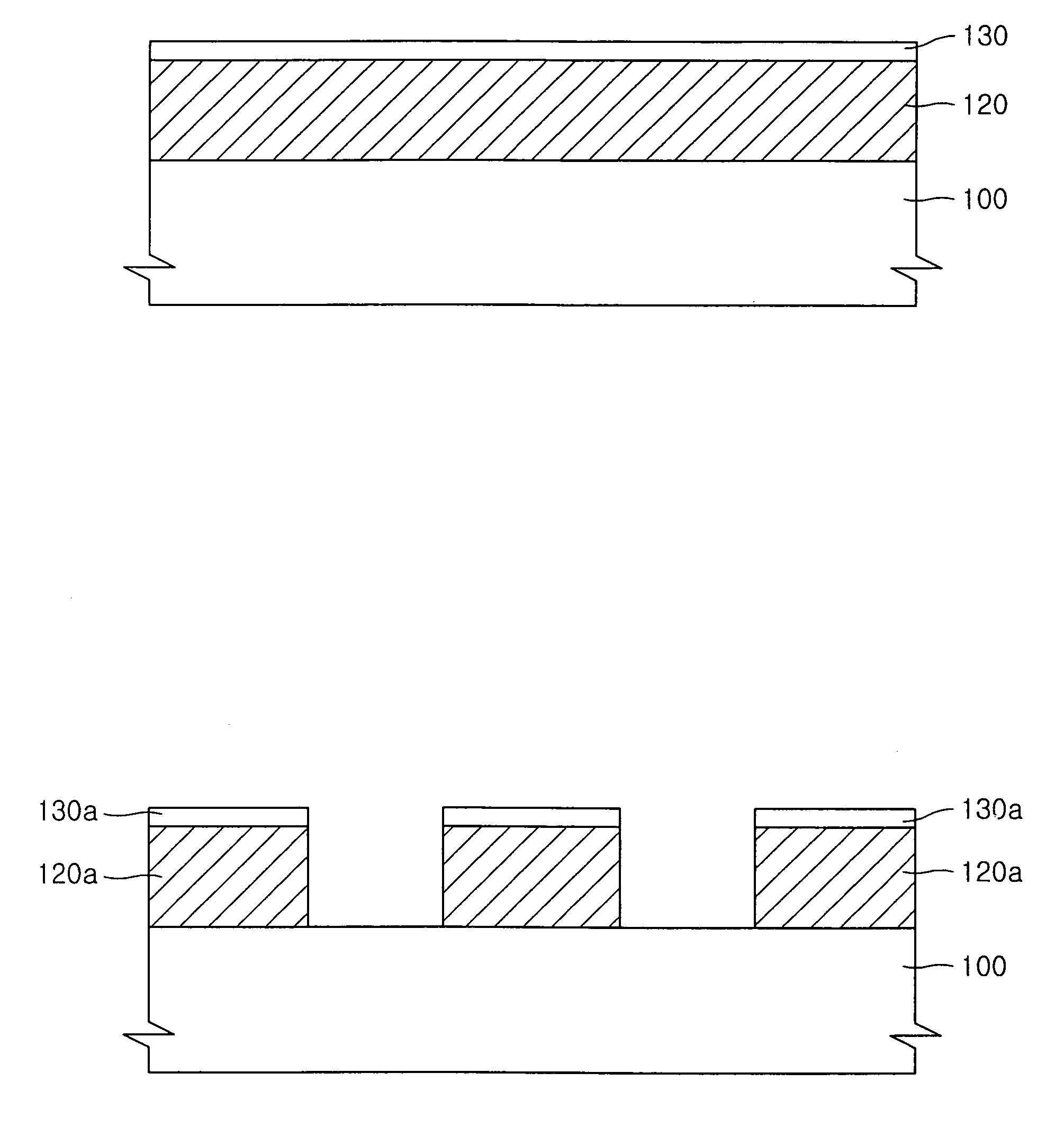
[0025]FIGS. 3A through 3F are cross-sectional views illustrating an exemplary method of forming a planarized, inter-metal insulation film in a semiconductor device according to one embodiment of the invention.

[0026] Referring to FIG. 3A, a metal layer 120 formed from, for example, aluminum, tungsten, copper, or an alloy of same, is formed on semiconductor substrate 100 to a predetermined first thickness. As noted above, an inter-layer insulation film (not shown) covering sub-structures formed on semiconductor substrate 10 might be interposed between these two layers, but...


PUM

PropertyMeasurementUnit
dielectric constantaaaaaaaaaa
temperaturesaaaaaaaaaa
temperatureaaaaaaaaaa

Abstract

A method for forming a planarized inter-metal insulation film is provided. The method includes applying a CMP process to an insulation film as controlled by a polish-stop layer pattern formed on an underlying metal wiring pattern. A PAE based material may be used to form the polish-stop layer.

Description

BACKGROUND OF THE INVENTION [0001] 1. Field of the Invention [0002] Embodiments of the invention relate to a method for manufacturing semiconductor devices. More particularly, embodiments of the invention relate to a method for forming a planarized inter-metal insulation film on a metal wiring layer. [0003] This application claims the benefit of Korean Patent Application No. 10-2005-0000377, filed on Jan. 4, 2005, the disclosure of which is hereby incorporated by reference in its entirety. [0004] 2. Description of the Related Art [0005] The various manufacturing processes used to fabricate semiconductor devices include numerous individual processes. Some of the individual processes relate to photolithography, etching, thin film formation, diffusion, planarization, etc. As repeatedly applied in constructive combination to a semiconductor substrate, these processes ultimately form, amongst other potential structures, conductive patterns separated by insulation films. [0006] The planar...

Claims


Application Information

Patent Timeline
Patent Type & Authority Applications(United States)
IPC IPC(8): H01L21/302H01L21/461
CPCH01L21/31053H01L21/31058H01L21/76819H01L21/304
Inventor YUN, SE-RAHHONG, CHANG-KILEE, JAE-DONG
Owner SAMSUNG ELECTRONICS CO LTD
Why Eureka
Try Eureka