Method and structure to reduce contact resistance on thin silicon-on-insulator device

a technology of metal oxidesilicon and contact resistance, which is applied in the direction of semiconductor devices, electrical equipment, basic electric elements, etc., can solve the problems of increasing the gap between the gate-to-source and drain overlap capacitance (miller capacitance), increasing the difficulty in forming low-series resistance source-drain contacts, and increasing the difficulty in avoiding silicidation of the source-drain diffusion from extending completely through the soi to the back oxide (or buried oxide),

Inactive Publication Date: 2007-11-01
GLOBALFOUNDRIES INC
View PDF4 Cites 14 Cited by
  • Summary
  • Abstract
  • Description
  • Claims
  • Application Information

AI Technical Summary

Benefits of technology

[0012] The present invention provides a robust method of precisely controlling the silicide depth in the source-drain region of a MOSFET, thus avoiding silcidation consuming the entire source-drain diffusion. The method assures than an unsilicided region remains in the interior of the source-drain. Thus, the interface area between the silicide and a single crystal silicon is increased and the series resistance is reduced.
[0013] In accordance with an exemplary aspect of the present invention, the method of reducing contact resistance on a silicon-on-insulator device includes exposing the sidewalls of the source / drain regions, forming porous silicon within a surface region of the source / drain, implanting dopants and forming silicide. An alternative approach is to selectively thicken the exposed source and drain regions after exposing the sidewalls of the source-drain regions by epitaxial-growth with an in-situ p+ doping. Subsequent anodization of the p+ epitaxial layer forms a porous layer of very well controlled thickness.
[0014] Furthermore, the present invention provides a process for forming dummy spacers with a predetermined width for the purpose of avoiding silicide spiking into the junction area.
[0015] Additionally, another feature of the invention is to remove spacers that would otherwise cover the sidewalls of the exposed source-drain islands, thus increasing the source-drain diffusion area available for introducing dopant and for forming contacts.

Problems solved by technology

However, a consequence of thinner (less than about 30 nm) SOI is increased difficulty in forming low-series resistance source-drain contacts.
Not only does the thinner SOI reduce the cross-sectional area normal to the current, but it becomes increasingly difficult to avoid silicidation of the source-drain diffusions from extending completely through the SOI to the back (or buried) oxide (BOX).
A method for forming raised source / drain involves epitaxial-growth, which leads to increasing the gate-to-source and drain overlap capacitance (Miller capacitance) and degraded performance.

Method used


Image

  • Method and structure to reduce contact resistance on thin silicon-on-insulator device
  • Method and structure to reduce contact resistance on thin silicon-on-insulator device
  • Method and structure to reduce contact resistance on thin silicon-on-insulator device

Examples


Embodiment Construction

[0019] Referring now to the drawings, and more particularly to FIGS. 1-15, there are shown exemplary embodiments of the method and structures according to the present invention.

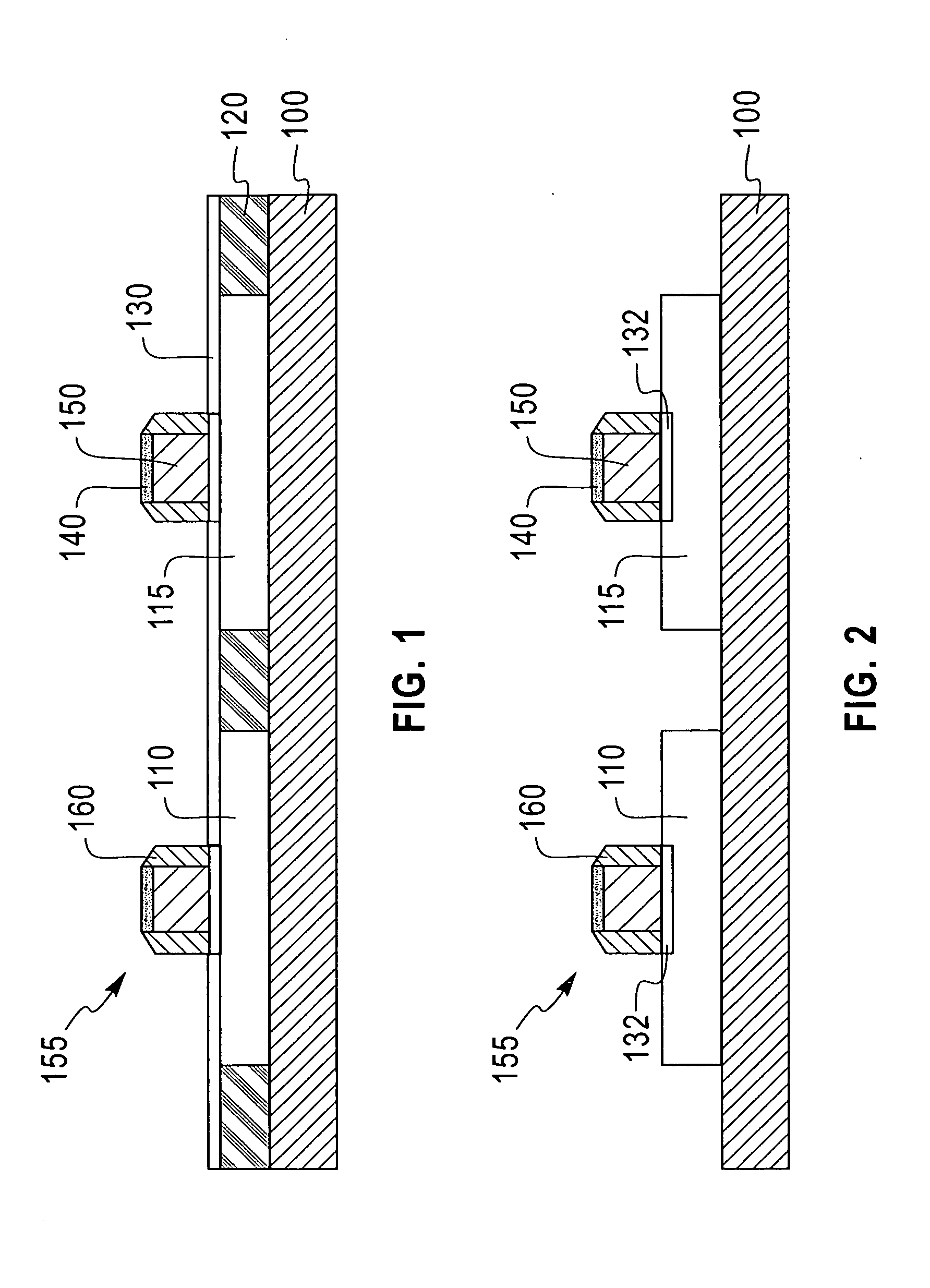
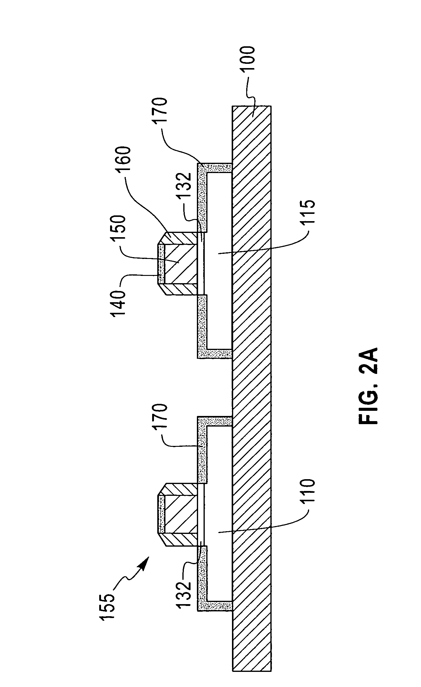
[0020]FIGS. 1-14 illustrate an exemplary method of forming a MOSFET while controlling the silicide depth in the source / drain region of the MOSFET in accordance with certain embodiments of the present invention.

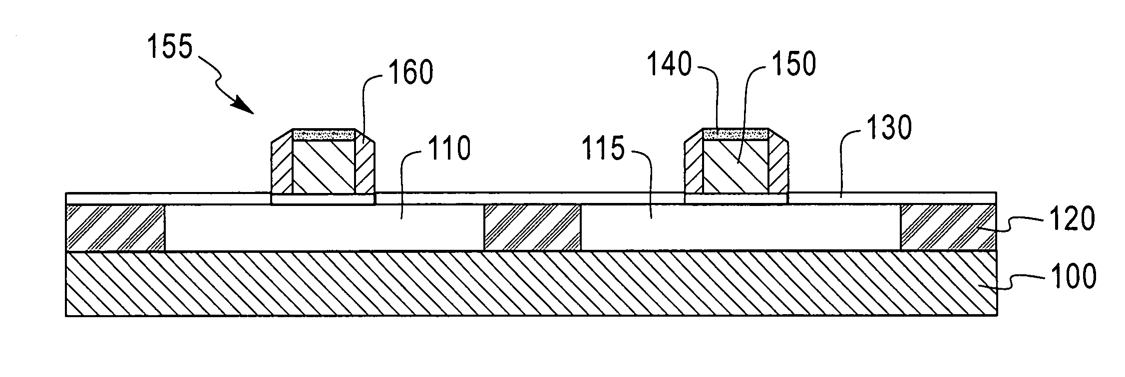
[0021] First, as depicted in FIG. 1, a low-k material (e.g., such as chemical vapor deposition (CVD) SiCOH, and spin-on low-k polymer material including SiLK and JSR porous low-k polymer, etc.) is used to form a sacrificial shallow trench isolation 120 on a silicon-on-insulator (SOI) wafer having a buried oxide layer 100. The bodies on the SOI wafer, which form pMOS 115 and nMOS 110, are properly doped. That is, doped to form a fully depleted body with a dopant concentration (p-type for NMOS and n-type for PMOS) of about 1E17 / cm3. Boron is an exemplary dopant for the PMOS and phosphorous and arsenic a...


PUM


Abstract

A method (and system) of reducing contact resistance on a silicon-on-insulator device, including controlling a silicide depth in a source-drain region of the device.

Description

BACKGROUND OF THE INVENTION [0001] 1. Field of the Invention [0002] The present invention generally relates to a method and apparatus for reducing contact resistance, and more particularly to a method and apparatus for reducing source / drain series resistance in an ultra-thin silicon-on-insulator metal-oxide-silicon field effect transistor. [0003] 2. Description of the Related Art [0004] As silicon-on-insulator (SOI) metal-oxide-silicon field effect transistor (MOSFET) channel lengths continue to be aggressively scaled from the 65 nm to the 45 nm node and beyond, it is necessary to reduce the SOI film thickness to suppress short channel effects. However, a consequence of thinner (less than about 30 nm) SOI is increased difficulty in forming low-series resistance source-drain contacts. Not only does the thinner SOI reduce the cross-sectional area normal to the current, but it becomes increasingly difficult to avoid silicidation of the source-drain diffusions from extending completely ...

Claims


Application Information

Patent Timeline
Patent Type & Authority Applications(United States)
IPC IPC(8): H01L21/28
CPCH01L29/458H01L29/66772H01L29/66628
Inventor GREENE, BRIAN J.HSU, LOUIS LU-CHENMANDELMAN, JACK ALLANSUNG, CHUN-YUNG
Owner GLOBALFOUNDRIES INC
Why Eureka
Try Eureka