ß-Ga2o3 single crystal growing method, thin-film single crystal growing method, Ga2o3 light-emitting device, and its manufacturing method

a single crystal growing and manufacturing method technology, applied in the direction of polycrystalline material growth, crystal growth process, chemically reactive gas, etc., can solve the problems of difficult control of crystal growth, difficult to grow single crystals in size, and difficult to obtain light-emitting devices emitted light having a shorter wavelength, etc., to achieve good workability, reduce cracking and twinning, and improve the effect of crystallinity

Inactive Publication Date: 2006-07-13
WASEDA UNIV
View PDF10 Cites 86 Cited by
  • Summary
  • Abstract
  • Description
  • Claims
  • Application Information

AI Technical Summary

Benefits of technology

The patent text describes a new material that has improved properties. It is more durable and can be worked more easily. This is achieved by reducing its tendency to crack and twin, while increasing its crystallinity.

Problems solved by technology

The technical problem addressed in this patent text is the difficulty in controlling crystal growth and the formation of cracks in a β-Ga2O3 single crystal growing method. Additionally, the text aims to provide a method for growing a thin-film single crystal with high quality and a Ga2O3 light-emitting device capable of emitting a light with a shorter wavelength than that in the ultraviolet region.

Method used


Image

  • ß-Ga2o3 single crystal growing method, thin-film single crystal growing method, Ga2o3 light-emitting device, and its manufacturing method
  • ß-Ga2o3 single crystal growing method, thin-film single crystal growing method, Ga2o3 light-emitting device, and its manufacturing method
  • ß-Ga2o3 single crystal growing method, thin-film single crystal growing method, Ga2o3 light-emitting device, and its manufacturing method

Examples


first embodiment

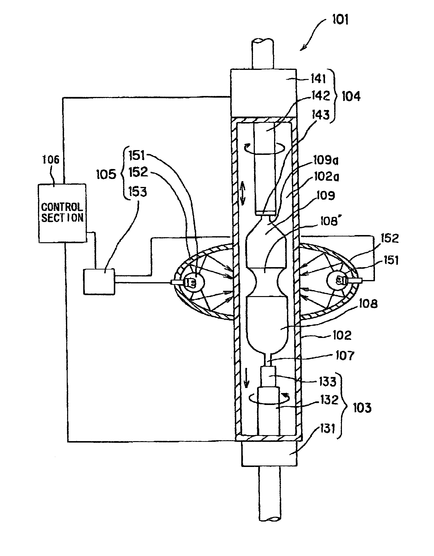
[0052]FIG. 1 shows infrared heating single crystal manufacturing equipment according to the first embodiment of the invention wherein the infrared heating single crystal manufacturing equipment 101 is used for manufacturing a β-Ga2O3 single crystal in accordance with a FZ method, and the equipment is schematically composed of a silica tube 102, a seed rotation section 103 for holding / rotating a β-Ga2O3 seed crystal (hereinafter referred to as “seed crystal”) 107, a raw material rotation section 104 for holding / rotating a β-Ga2O3 polycrystalline raw material (hereinafter referred to as simply “polycrystalline raw material”) 109, a heating section 105 for heating the polycrystalline raw material 109 to melt it, a seed rotation section 103, and a control section 106 for controlling the raw material rotation section 104 and the heating section 105.

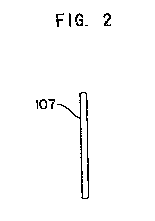
[0053] The seed rotation section 103 is provided with a seed chuck 133 for holding the seed crystal 107, a lower rotary shaft 132 for transm...

second embodiment

[0082]FIG. 7 shows a schematic constitution of film formation equipment according to a second embodiment of the invention, The film formation equipment 201 performs the film formation in accordance with PLD method and which is provided with a chamber 202 containing a space 220 which can be evacuated, a target table 205 placed in the chamber 202, a target 203 being maintained on the target table, a rotation mechanism 211 placed outside the chamber 202 and for rotating the target table 205, a substrate holding section 207 placed inside the chamber 202 and for holding a substrate 206, a heater which can heat the substrate 206 up to 1500° C. being housed in the substrate holding section, a radical injection section 208 for injecting radicals into the chamber 202 through a pipe 202a, an exhaust section 209 having a vacuum pump (not shown) for exhausting the space 220 through a pipe 202b to evacuate the space 220, and a laser section 204 provided outside the chamber202 and for irradiating...

third embodiment

[0093]FIG. 8 shows a section of a MIS type light-emitting device according to a third embodiment of the present invention. The MIS type light-emitting device 260 is provided with a substrate 206 made of a β-Ga2O3 single crystal, a β-Ga2O3 thin-film single crystal 261 exhibiting an n-type conductivity and formed on the top of the substrate 206, an insulation layer 262 made of a β-Ga2O3 thin-film crystal and formed on the top of the n-type β-Ga2O3 thin-film single crystal 261, a gold electrode 263 formed on the top of the insulation layer 262, a bonding 267 attached on the top of the gold electrode 263 and to which a lead 268 is connected, an n-electrode 264 formed on the bottom of the substrate 206, and a bonding 265 attached to the bottom of the n-electrode 264 and to which a lead 266 is connected.

[0094] The insulation layer 262 is formed by annealing the β-Ga2O3 crystal at 900° C. in an oxygen atmosphere with no oxygen defect in the surface of 10 to 1000 nm.

[0095] According to th...


PUM


Abstract

A method for growing a β-Ga2O3 single crystal hardly cracking and having a weakened twinning tendency and an improved crystallinity, a method for growing a thin-film single crystal with high quality, a GazO3 light-emitting device capable of emitting a light in the ultraviolet region, and its manufacturing method are disclosed. In an infrared-heating single crystal manufacturing system, a seed crystal and polycrystalline material are rotated in mutually opposite directions and heated, and a β-Ga2O3 single crystal is grown in one direction selected from among the a-axis <100> direction, the b-axis <010> direction, and the c-axis <001> direction. A thin film of a β-Ga2O3 single crystal is formed by PLD. A laser beam is applied to a target to excite atoms constituting the target Ga atoms are released from the target by thermal and photochemical actions. The free Ga atoms are bonded to radicals in the atmosphere in the chamber. Thus, a thin film of a β-Ga2O3 single crystal is grown on a substrate of a β-Ga2O3 single crystal A light-emitting device comprises an n-type substrate produced by doping a β-Ga2O3 single crystal with an n-type dopant and a p-type layer produced by doping the β-Ga2O3 single crystal with a p-type dopant and junctioned to the top of the n-type substrate. The light-emitting device emits a light from the junction portion.

Description


Claims


Application Information

Patent Timeline
Owner WASEDA UNIV
Why Eureka
Try Eureka