Method of forming a thin wafer stack for a wafer level package

Inactive Publication Date: 2005-12-22
SAMSUNG ELECTRONICS CO LTD
View PDF3 Cites 116 Cited by
  • Summary
  • Abstract
  • Description
  • Claims
  • Application Information

AI Technical Summary

Benefits of technology

[0018] According to the invention, when the wafer with the integrated circuit is processed to reduce the thickness of the wafer, and when the resultant thin wafer is treated, warping of the thin wafer can be prevented. Accordingly,

Problems solved by technology

However, it is very difficult to reduce the chip's thickness via a wafer thinning process.
A warped wafer is very difficult to process, as required, since wafer processing assumes good wafer plan

Method used


Image

  • Method of forming a thin wafer stack for a wafer level package
  • Method of forming a thin wafer stack for a wafer level package
  • Method of forming a thin wafer stack for a wafer level package

Examples


Embodiment Construction

[0035] The invention will now be described more fully with reference to the accompanying drawings, in which exemplary embodiments of the invention are shown. The invention may, however, be embodied in many different forms and should not be construed as being limited to the embodiments set forth herein; rather, these embodiments are provided so that this disclosure will be thorough and complete, and will fully convey the concept of the invention to those skilled in the art.

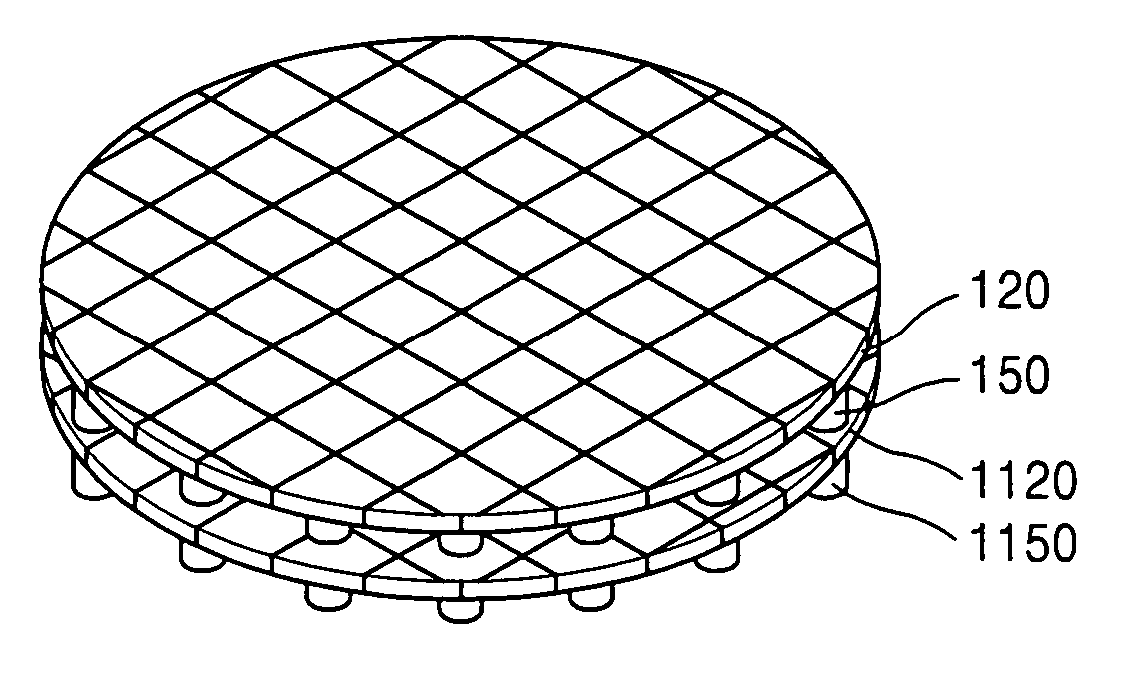
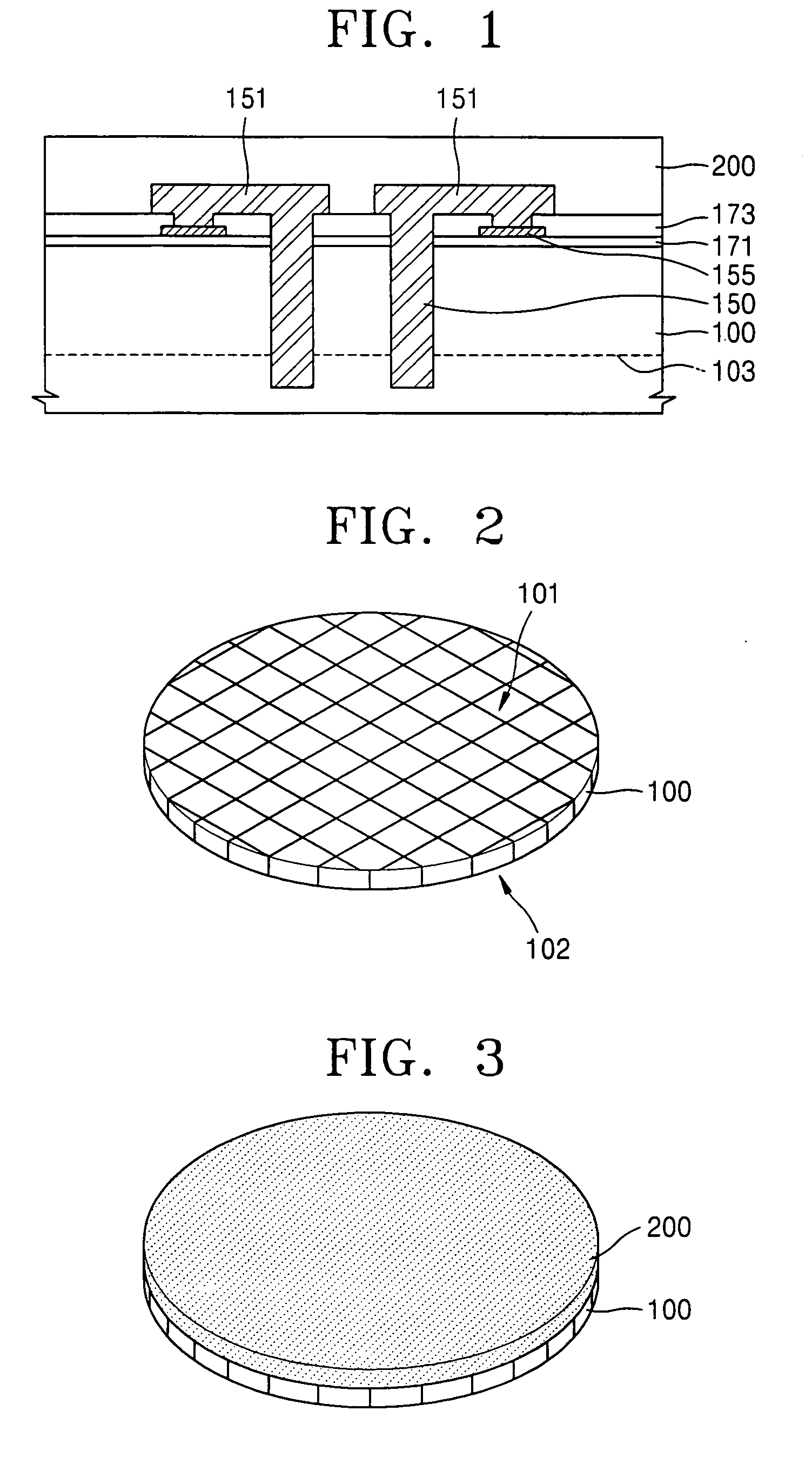
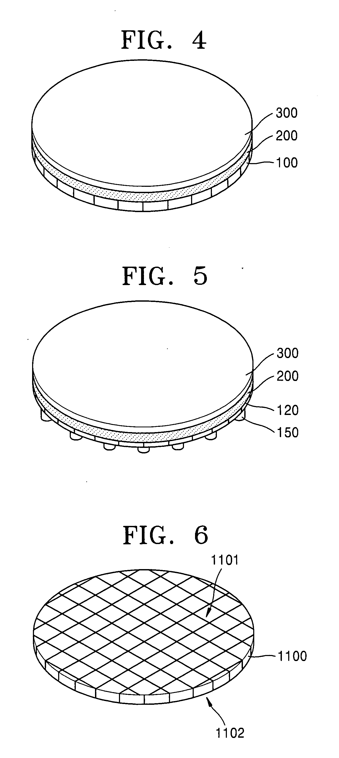
[0036] In order to form a wafer level package, the invention forms a wafer stack in which thin wafers are connected to one another by electrically connecting one or more conductive bumps to one or more corresponding conductive connection pads. Before the wafer with an integrated circuit is stacked, the wafer is thinned by back-grinding and / or etching a back surface thereof to have a small thickness, for example, of only approximately several tens of μm.

[0037] By greatly reducing the wafer's thickness before the w...


PUM


Abstract

A method of forming a stack of thin wafers provides a wafer level stack to greatly reduce process time compared to a method where individually separated chips are stacked after a wafer is sawed. A rigid planar wafer support member stabilizes and planarizes each wafer while it is thin or its thickness is reduced and during subsequent wafer processing. Thinned wafers are stacked and the external support members are removed by applying heat or ultraviolet (UV) light to an expandable adhesive layer between the support members and the thin wafers. The stacked wafers then can be further processed and packaged without thin-wafer warping, cracking or breaking. A wafer level package made in accordance with the invented method also is disclosed.

Description

BACKGROUND OF THE INVENTION [0001] This application claims the priority of Korean Patent Application No. 2004-46558, filed on Jun. 22, 2004, in the Korean Intellectual Property Office, the disclosure of which is incorporated herein in its entirety by reference. [0002] 1. Field of the Invention [0003] The invention relates to a method of manufacturing a semiconductor, and more particularly, to a method of forming a wafer stack to employ in a wafer level package. [0004] 2. Description of the Related Art [0005] At present, various methods of packaging a semiconductor device chip of an integrated circuit are provided in a semiconductor manufacture technology. Many semiconductor device packaging technologies require a thin chip having a thickness of several tens of μm for high density integration. [0006] For example, in a manufacture technology relating to multi-chip packaging (MCP) or multi-stack packaging (MSP), very thin chips are required to make chip stacks. Further, when an ultra-t...

Claims


Application Information

Patent Timeline
IPC IPC(8): H01L21/44H01L21/4763H01L21/48H01L21/50H01L23/12H01L21/60H01L21/68H01L21/98H01L23/48H01L25/065
CPCH01L21/6835H01L23/481H01L2224/2919H01L2924/3025H01L2924/01079H01L24/81H01L24/83H01L25/0657H01L25/50H01L2221/6834H01L2224/16H01L2224/8121H01L2224/81815H01L2224/83851H01L2225/06513H01L2225/06541H01L2924/3512H01L2924/00H01L2924/00014H01L2924/14H01L2224/05024H01L2224/02372H01L2224/05009H01L2224/05022H01L2224/05548H01L2224/05001H01L2224/05124H01L2224/05144H01L2224/05147H01L2224/02377H01L24/05H01L2224/05599H01L23/12
Inventor HWANG, HYEONJEONG, KI-KWON
Owner SAMSUNG ELECTRONICS CO LTD
Why Eureka
Try Eureka