Back side contact structure for a semiconductor device and corresponding manufacturing process

a back side contact and semiconductor technology, applied in the direction of semiconductor devices, electrical apparatus, transistors, etc., can solve the problems of reliability, possible failure or drop in production yield, and the cost and unproductive methods of setting up a good electrical contact, so as to reduce the thickness of the wafer and increase the total thickness of the back side metallization. , good electrical contact

Pending Publication Date: 2022-08-04
STMICROELECTRONICS SRL
View PDF4 Cites 0 Cited by
  • Summary
  • Abstract
  • Description
  • Claims
  • Application Information

AI Technical Summary

Benefits of technology

[0015]Various embodiments disclosed herein overcome the drawbacks of previous solutions by providing an improved solution that represents a good compromise between management of the stress caused by the back side metal stack and the electrical properties of the semiconductor device, in particular ensuring a good electrical contact with the substrate, taking into account the reduction of the thickness of the wafer and the desire to increase the total thickness of the back side metallization.

Problems solved by technology

A problem regarding the back side metal stack is the high bending induced on the wafer, especially in the case of thin wafers (<100 μm), which causes handling problems in the final manufacturing steps and problems of reliability of the resulting devices, with possible failure or drops in production yield.
Furthermore, for some devices, setting up a good electrical contact involves costly and unproductive methods to limit the temperature reached by the wafer in each one of the deposition steps involved in the formation of the back side metal stack.
The present Applicant has found that the solutions currently used have, however, some limitations and suffer from some drawbacks, in particular due to a reduction, even considerable, of the production efficiency, and to an inadequate management of the stress caused by the metal stack.

Method used


Image

  • Back side contact structure for a semiconductor device and corresponding manufacturing process
  • Back side contact structure for a semiconductor device and corresponding manufacturing process
  • Back side contact structure for a semiconductor device and corresponding manufacturing process

Examples


Embodiment Construction

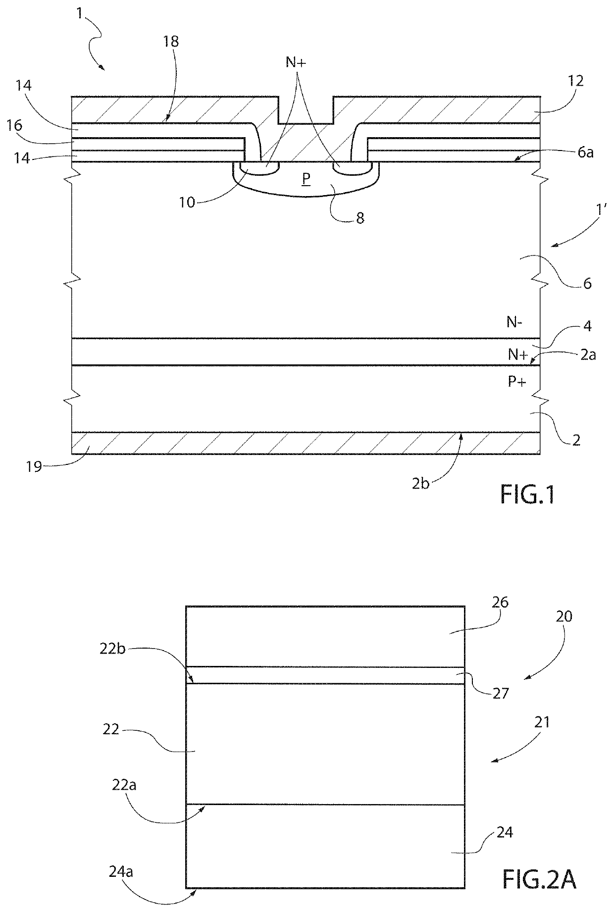
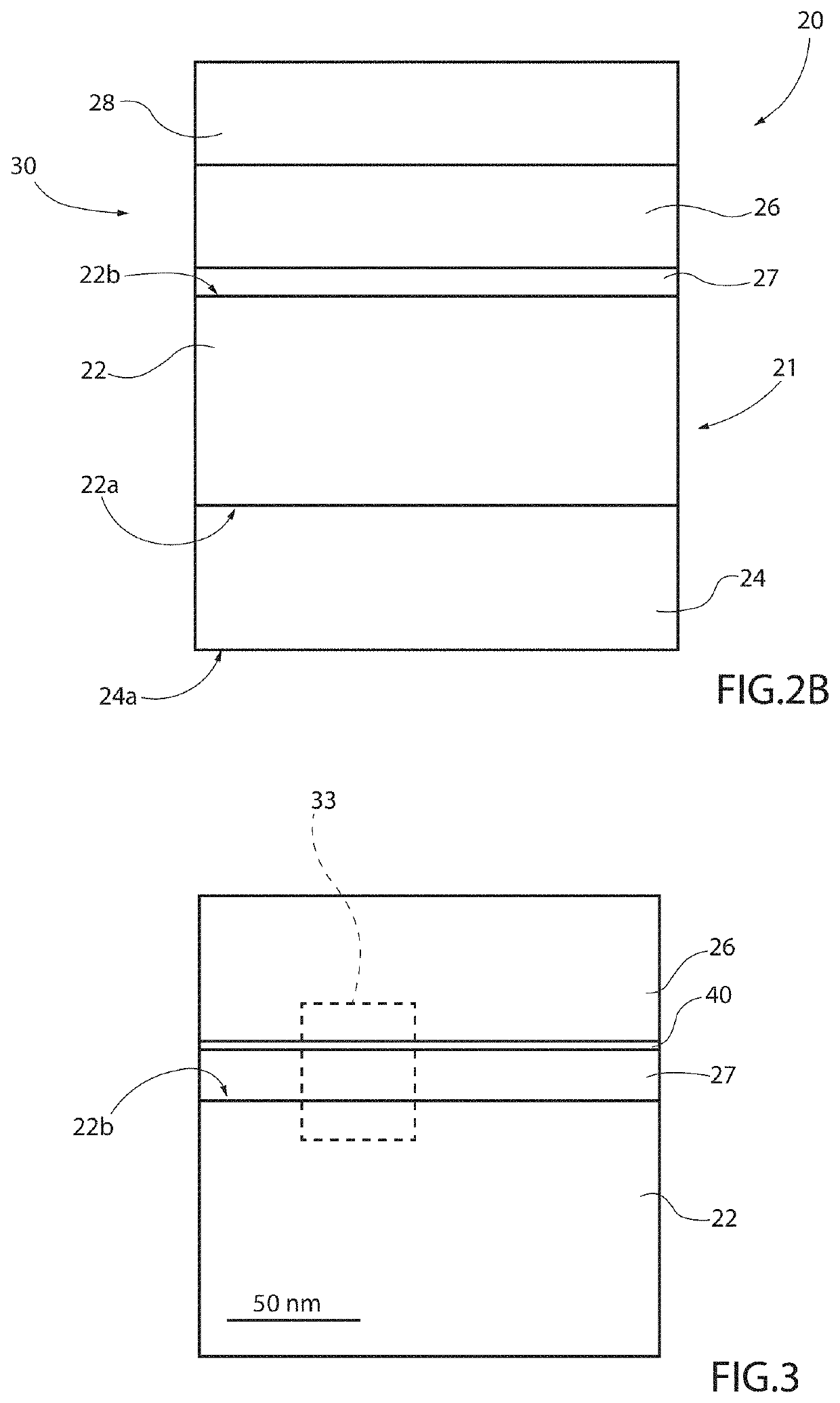
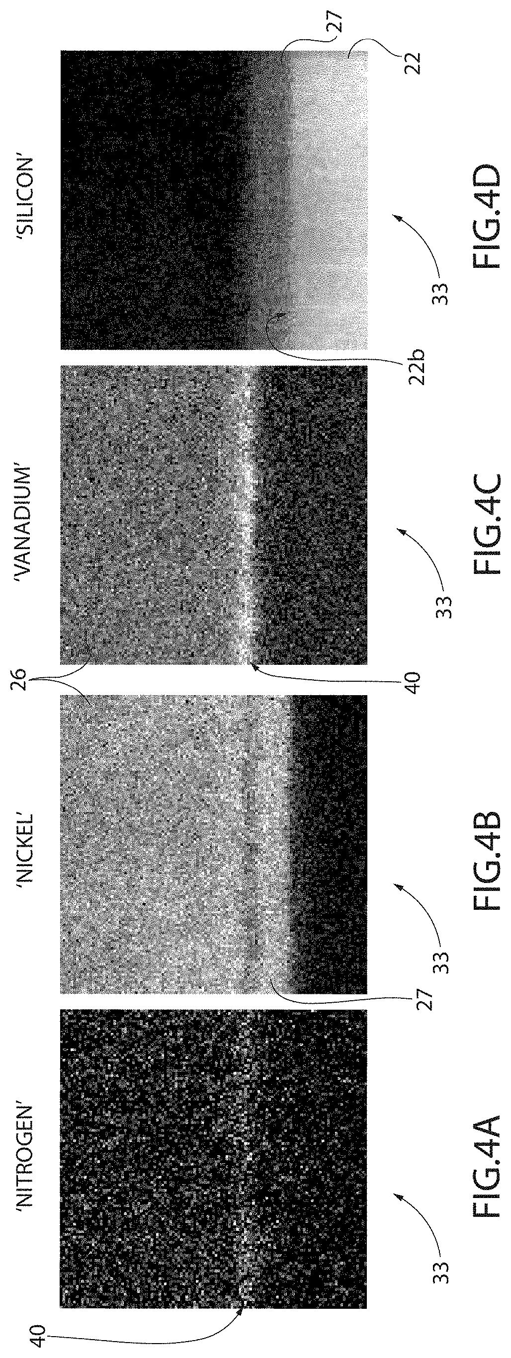
[0022]As will be described in detail hereinafter, an aspect of the present solution envisages an alternative embodiment of a back side metal structure (or stack), on the rear side of the substrate or wafer of a semiconductor device, in particular a silicon-based semiconductor device, for example, a device used for power applications.

[0023]This alternative embodiment envisages overlapping of just two metal layers on the aforesaid rear side of the substrate.

[0024]In particular, a first metal layer, in contact with the substrate, in this case itself constitutes an active soldering layer and is formed by a deposition (in particular PVD) technique and a deposition process such as to ensure concurrent formation of a silicide region, the silicide being a binary compound formed by atoms of metal and silicon, in direct contact with the substrate. This silicide region ensures good electrical contact with the substrate and moreover guarantees a good mechanical strength.

[0025]In this solution, ...


PUM

PropertyMeasurementUnit
thicknessaaaaaaaaaa
thicknessaaaaaaaaaa
thicknessaaaaaaaaaa

Abstract

Various embodiments provide a vertical-conduction semiconductor device that includes: a silicon substrate having a front face and a rear face; a front-side structure arranged on the front face of the substrate, having at least one current-conduction region at the front face; and a back side metal structure, arranged on the rear face of the substrate, in electrical contact with the substrate and constituted by a stack of metal layers. The back side metal structure is formed by: a first metal layer; a silicide region, interposed between the rear face of the substrate and the first metal layer and in electrical contact with the aforesaid rear face; and a second metal layer arranged on the first metal layer.

Description

BACKGROUNDTechnical Field[0001]The present solution relates to an improved back side contact structure for a semiconductor device and to a corresponding manufacturing process.Description of the Related Art[0002]Several vertical-conduction semiconductor devices, in particular silicon-based devices for power applications, have a contact or metallization on the back or back side; for example, MOSFET (metal oxide semiconductor field-effect transistor) transistor devices of a VDMOS (Vertical Double-Diffused Metal Oxide Semiconductor) type or transistor devices of an IGBT (Insulated Gate Bipolar Transistor) type are known, in which a flow of current occurs in a vertical direction in the device, towards an electrical contact on the back side.[0003]In this regard, and purely by way of example, FIG. 1 shows, in cross-sectional view, an IGBT (insulated gate bipolar transistor) transistor device 1 with planar configuration, comprising a wafer 1′ including a substrate 2, of silicon, for example...

Claims


Application Information

Patent Timeline
Patent Type & Authority Applications(United States)
IPC IPC(8): H01L29/417H01L29/66H01L29/739H01L29/40H01L29/45
CPCH01L29/41708H01L29/66333H01L29/456H01L29/401H01L29/7395H01L29/7802H01L21/28518
Inventor RENNA, CROCIFISSO MARCO ANTONIOLANDI, ANTONIOCAFRA, BRUNELLA
Owner STMICROELECTRONICS SRL
Why Eureka
Try Eureka