Method for forming interconnects on thin wafers

a technology of interconnects and thin wafers, applied in the direction of metal working equipment, manufacturing tools, soldering apparatus, etc., can solve the problems of damage to semiconductor chips, and achieve the effects of reducing the thickness of the wafer

Inactive Publication Date: 2005-10-04
IBM CORP
View PDF13 Cites 2 Cited by
  • Summary
  • Abstract
  • Description
  • Claims
  • Application Information

AI Technical Summary

Benefits of technology

[0005]A first aspect of the present invention is a method of forming a semiconductor interconnect comprising, in the order recited: (a) providing a semiconductor wafer; (b) forming bonding pads in a terminal wiring level on the frontside of the wafer; (c) reducing the thickness of the wafer; (d) forming solder bumps on the bonding pads; and (e) dicing the wafer into bumped semiconductor chips.
[0006]A second aspect of the present invention is a method of forming a semiconductor interconnect comprising, in the order recited: (a) providing a semiconductor wafer; (b) forming bonding pads in a terminal wiring level on the frontside of the wafer; (c) reducing the thickness of the wafer to produce a reduced thickness wafer; (d) providing an evaporation fixture comprising a bottom ring, a shim, an evaporation mask and a top ring; (e) placing the shim into the bottom ring; (f) placing the reduced thickness wafer on the shim; (g) placing on and aligning the mask to the reduced thickness wafer; (h) placing said top ring over said mask and temporarily fastening said top ring to said bottom ring; (i) evaporating solder bumps on the bonding pads through the mask; (j) removing the reduced thickness wafer from the fixture; and (k) dicing the reduced thickness wafer into bumped semiconductor chips.
[0007]A third aspect of the present invention is A fixture for holding wafer and an evaporative mask comprising: a bottom ring having a inner periphery and an outer periphery, the bottom ring having a raised inner lip formed along the inner periphery and a raised outer lip formed along the outer periphery, the height of the inner lip above a surface of the bottom ring being greater than a height of the outer lip above the surface of the bottom ring; a shim having a inner and an outer periphery, the outer periphery of the shim fitting inside and in proximity to the outer lip of the bottom ring, a bottom surface of the shim proximate to the inner periphery of the shim contacting an upper surface of the inner lip of the bottom ring; a top ring having an inner periphery and an outer periphery, the top ring having a lower raised lip formed along the inner periphery of the bottom ring and extending below a bottom surface of the top ring; and the bottom ring and the top ring adapted to press a bottom surface of the wafer against an upper surface of the shim and to press a top surface of the wafer against a bottom surface of the mask and to press a top surface of the mask proximate to the periphery of the mask against a lower surface of the lower raised lip of the top ring.

Problems solved by technology

Current methods of thinning semiconductor wafers often lead to damage of the semiconductor chips.

Method used


Image

  • Method for forming interconnects on thin wafers
  • Method for forming interconnects on thin wafers
  • Method for forming interconnects on thin wafers

Examples


Embodiment Construction

[0020]For the purposes of the present invention, the terms substrate and wafer may be used interchangeably.

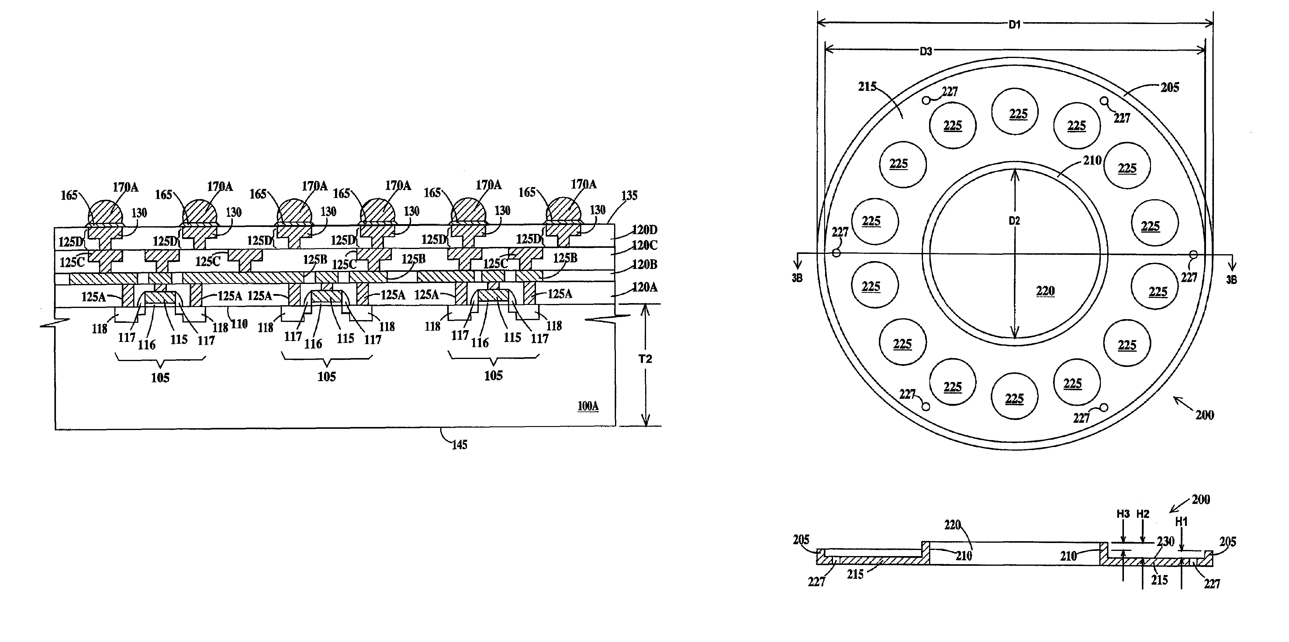
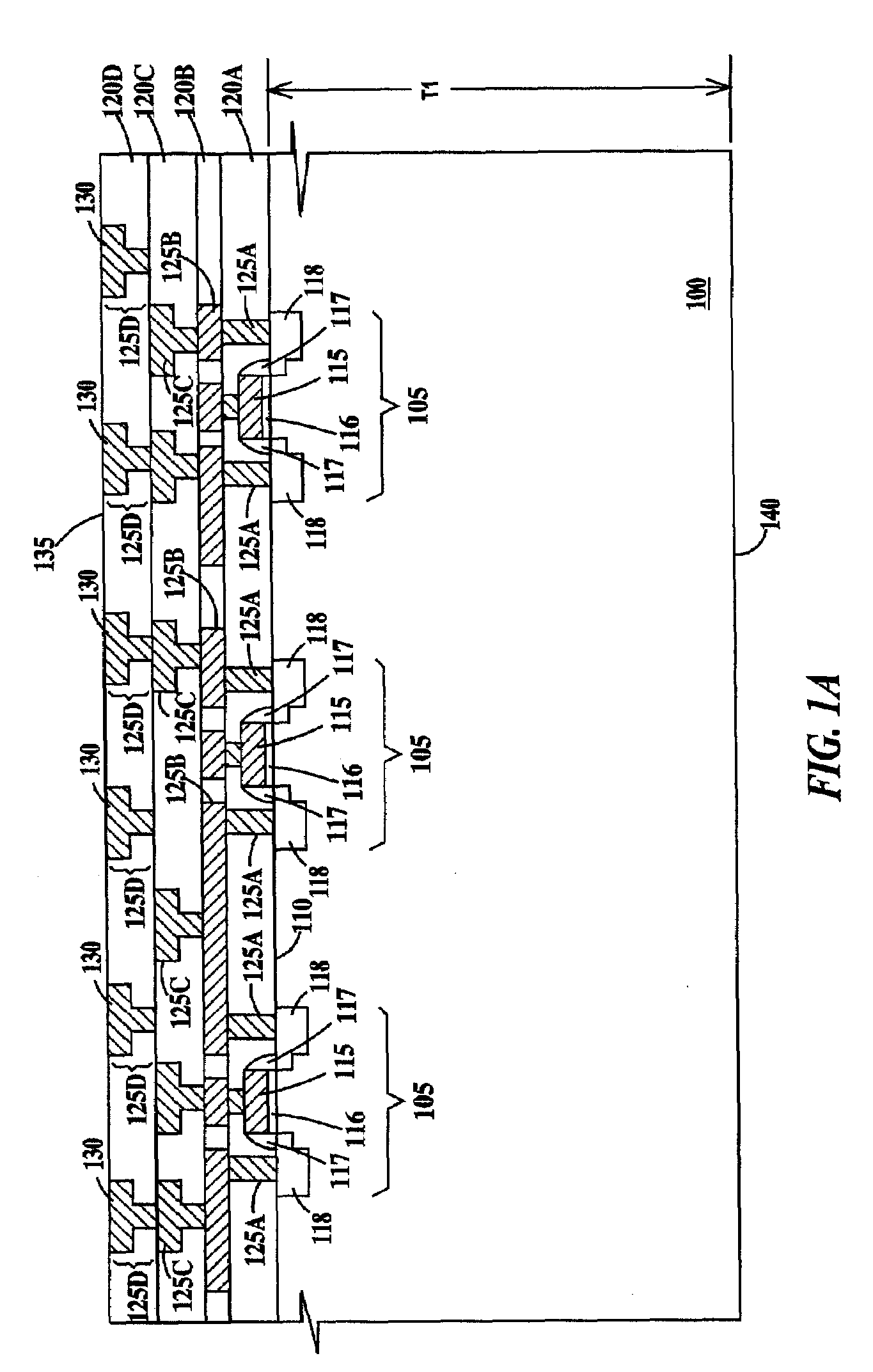
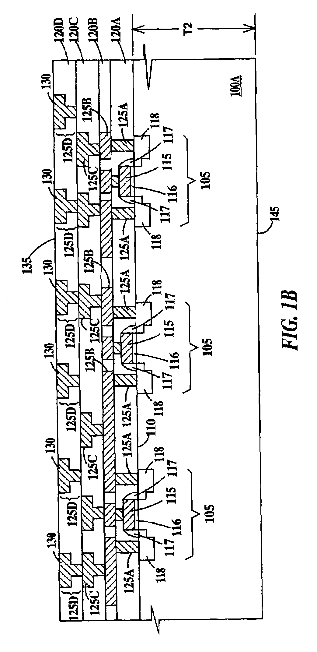
[0021]FIGS. 1A through 1F are partial cross-sectional views of the fabrication of a semiconductor wafer according to the present invention. In FIG. 1A, a substrate 100 such as a semiconductor bulk silicon substrate or a semiconductor silicon-on-insulator (SOI) substrate has a thickness T1. Formed in / on substrate 100 is a multiplicity of active Field effect transistors (FETs) 105. FETs 105 include gate electrodes 115 formed over gate dielectric formed 116 and between spacers 117 on a top surface 110 of substrate 100 and source / drains 118 formed in the substrate. FETs 105 are exemplary of devices and structures normally found in semiconductor circuits of semiconductor chips and many other structures and devices such as capacitors, resistors, inductors, bipolar transistors and diffused and dielectric isolation. FETs 105 are wired into circuits in a first wiring level 120A, a secon...


PUM


Abstract

A method of forming a semiconductor interconnect including, in the order recited: (a) providing a semiconductor wafer; (b) forming bonding pads in a terminal wiring level on the frontside of the wafer; (c) reducing the thickness of the wafer; (d) forming solder bumps on the bonding pads; and (e) dicing the wafer into bumped semiconductor chips.

Description

BACKGROUND OF INVENTION[0001]1. Field of the Invention[0002]The present invention relates to the field of semiconductor processing; more specifically, it relates to a method of forming a solder interconnect structure on a thin wafer.[0003]2. Background of the Invention[0004]Increasing density of semiconductor devices has allowed semiconductor chips to decrease in area. Along with the decrease in chip area, has come a need to make the semiconductor chips thinner. Current methods of thinning semiconductor wafers often lead to damage of the semiconductor chips.SUMMARY OF INVENTION[0005]A first aspect of the present invention is a method of forming a semiconductor interconnect comprising, in the order recited: (a) providing a semiconductor wafer; (b) forming bonding pads in a terminal wiring level on the frontside of the wafer; (c) reducing the thickness of the wafer; (d) forming solder bumps on the bonding pads; and (e) dicing the wafer into bumped semiconductor chips.[0006]A second as...

Claims


Application Information

Patent Timeline
Patent Type & Authority Patents(United States)
IPC IPC(8): H01L21/02H01L21/60
CPCB23K3/0623H01L24/03H01L24/05H01L24/11H01L24/74B23K2201/40H01L24/02H01L24/12H01L2224/0401H01L2224/05006H01L2224/05568H01L2224/05599H01L2224/11472H01L2224/13022H01L2224/13023H01L2224/16H01L2924/01006H01L2924/01013H01L2924/01014H01L2924/01022H01L2924/01029H01L2924/01042H01L2924/0105H01L2924/01074H01L2924/01079H01L2924/01082H01L2924/014H01L2924/04941H01L2924/19041H01L2924/19042H01L2924/19043H01L2224/05027H01L24/13H01L2221/68359H01L2224/0345H01L2224/05018H01L2224/05147H01L2224/05166H01L2224/05171H01L2224/05558H01L2224/05644H01L2224/05647H01L2224/1145H01L2224/11849H01L2224/13116H01L2224/742H01L2224/94H01L2924/00013H01L2924/01005H01L2924/01019H01L2224/05572H01L2924/0002H01L2924/1305H01L2924/00014H01L2224/11H01L2224/03H01L2224/13099H01L2224/05099H01L2224/13599H01L2224/29099H01L2224/29599H01L2924/00H01L2224/05552B23K2101/40
Inventor GARDECKI, LEONARD J.PALMER, JAMES R.PROBSTFIELD, ERIK M.WIRSING, ADOLF E.
Owner IBM CORP
Why Eureka
Try Eureka