Method and apparatus for handling thin semiconductor wafers

a technology processing methods, applied in the direction of electrical apparatus, semiconductor/solid-state device manufacturing, basic electric elements, etc., can solve the problems of reducing throughput, requiring thinner semiconductor devices, and high machinery costs, so as to reduce wafer thickness, safe handling of thin semiconductor wafers, and cost-effective and flexible

Inactive Publication Date: 2007-01-02
ADVANCED MICRO DEVICES INC
View PDF6 Cites 2 Cited by
  • Summary
  • Abstract
  • Description
  • Claims
  • Application Information

AI Technical Summary

Benefits of technology

[0008]An advantage of the present invention is a method and apparatus for safely handling thin semiconductor wafers. Another advantage of the present invention is a technique for reducing wafer thickness which is cost-effective and flexible.
[0009]According to the present invention, the foregoing and other advantages are achieved in part by a cassette for holding a thin semiconductor wafer, the cassette comprising a center support and a pair of opposed edge supports for supporting the wafer such that the wafer is substantially planar.
[0010]Another aspect of the present invention is a cassette for holding a thin semiconductor wafer, the cassette having a pair of opposed edge supports, each edge support comprising a substantially planar first part and a second part. The second part comprises a flattening section, substantially parallel to the first part and spaced from the first part to form a first gap between the first part and the flattening section. The flattening section is for cooperating with the first part to support the wafer such that the wafer is substantially planar. A wafer guiding section cooperates with the first part to guide the wafer into the first gap as the wafer is inserted into the cassette.
[0011]A still further aspect of the present invention is a method of reducing the thickness of a semiconductor wafer having an initial thickness, the method comprising grinding a back side of the wafer to reduce the initial thickness to an intermediate thickness, and plasma etching the back side of the wafer to reduce the intermediate thickness to a final thickness.
[0012]Additional advantages and other features of the present invention will be set forth in part in the description which follows and in part will become apparent to those having ordinary skill in the art upon examination of the following or may be learned from the practice of the invention. The advantages of the invention may be realized and obtained as particularly pointed out in the appended claims. As will be realized, the present invention is capable of other and different embodiments, and its several details are capable of modifications in various obvious respects, all without departing from the invention. Accordingly, the drawings and description are to be regarded as illustrative in nature, and not as restrictive.

Problems solved by technology

However, recently developed device packaging schemes; e.g., “chip-sized packages” used in miniaturized products such as cell phones, are significantly smaller than conventional packages, and require thinner semiconductor devices.
Such machinery is very expensive, and is only as fast as its slowest component.
Therefore, backgrinding is a “bottleneck” in wafer processing, reducing throughput and raising production costs.
A further disadvantage of conventional processes is that thin semiconductor wafers tend to warp and sag after backgrinding, due to backgrinding induced stresses and other mechanical stresses.
Moreover, when a fork attempts to remove a sagging and / or warped wafer from the cassette, the fork can easily hit the wafer and scratch or otherwise damage it, since the wafer is not within the “reference window” of a predetermined reference plane.
Thus, the fork cannot safely handle the thin wafer.

Method used


Image

  • Method and apparatus for handling thin semiconductor wafers
  • Method and apparatus for handling thin semiconductor wafers
  • Method and apparatus for handling thin semiconductor wafers

Examples


Embodiment Construction

[0019]Conventional methodologies for thinning semiconductor wafers are time-consuming, and require expensive dedicated equipment, which increases the cost of the finished device and reduces manufacturing throughput. Conventional methods for handling thin wafers result in damage to the wafers, reducing yield. The present invention addresses and solves these problems stemming from conventional manufacturing processes.

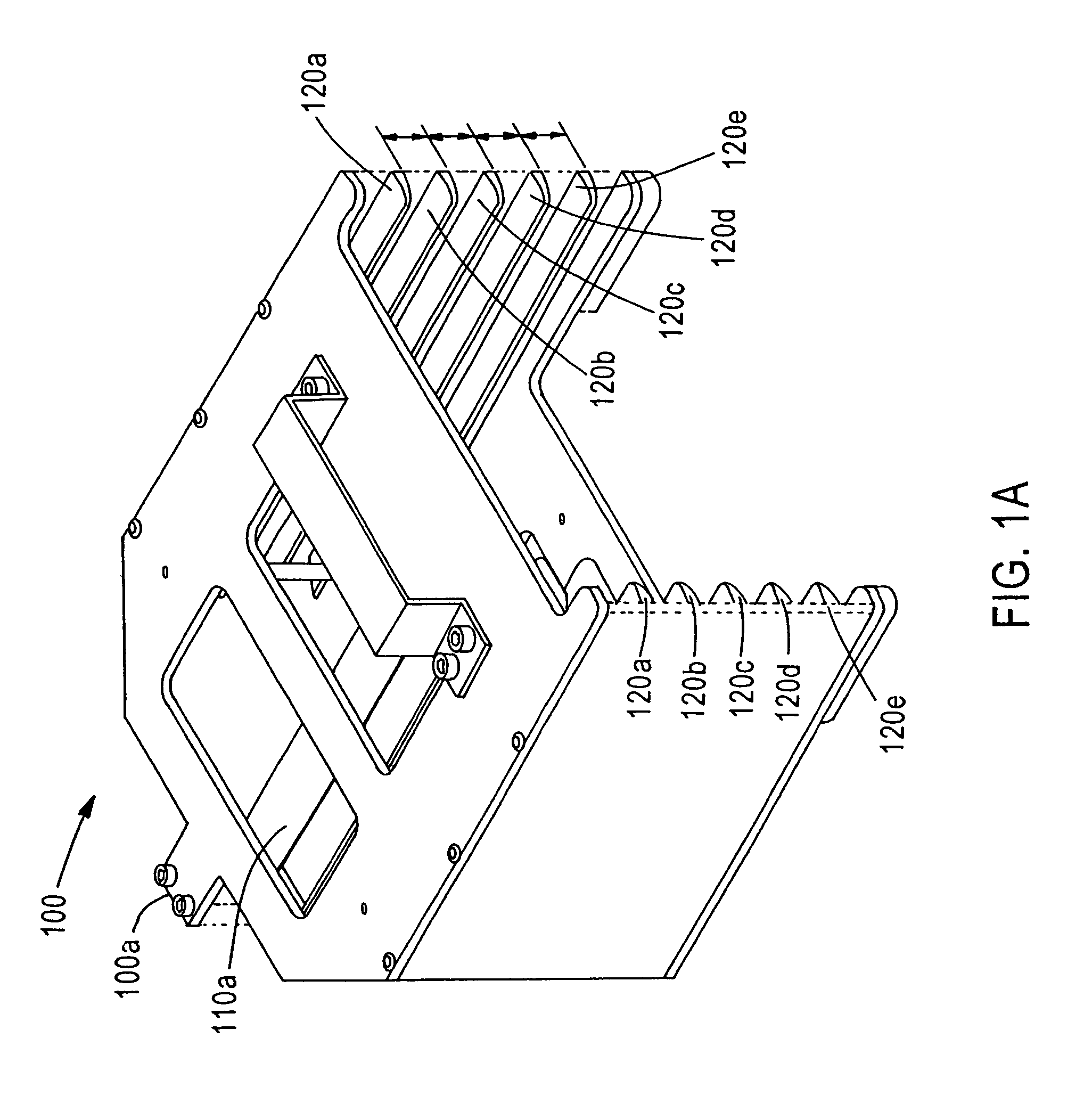
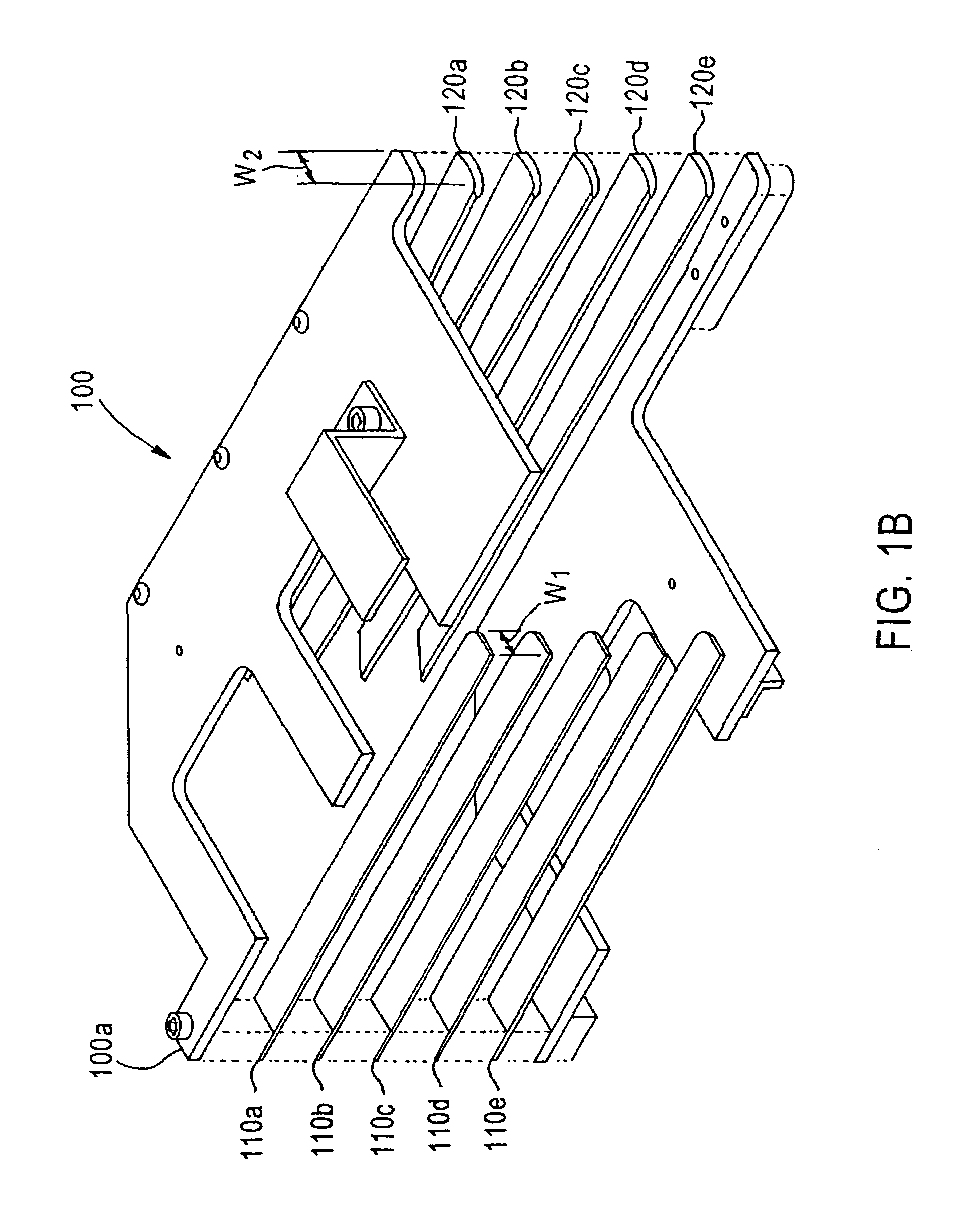
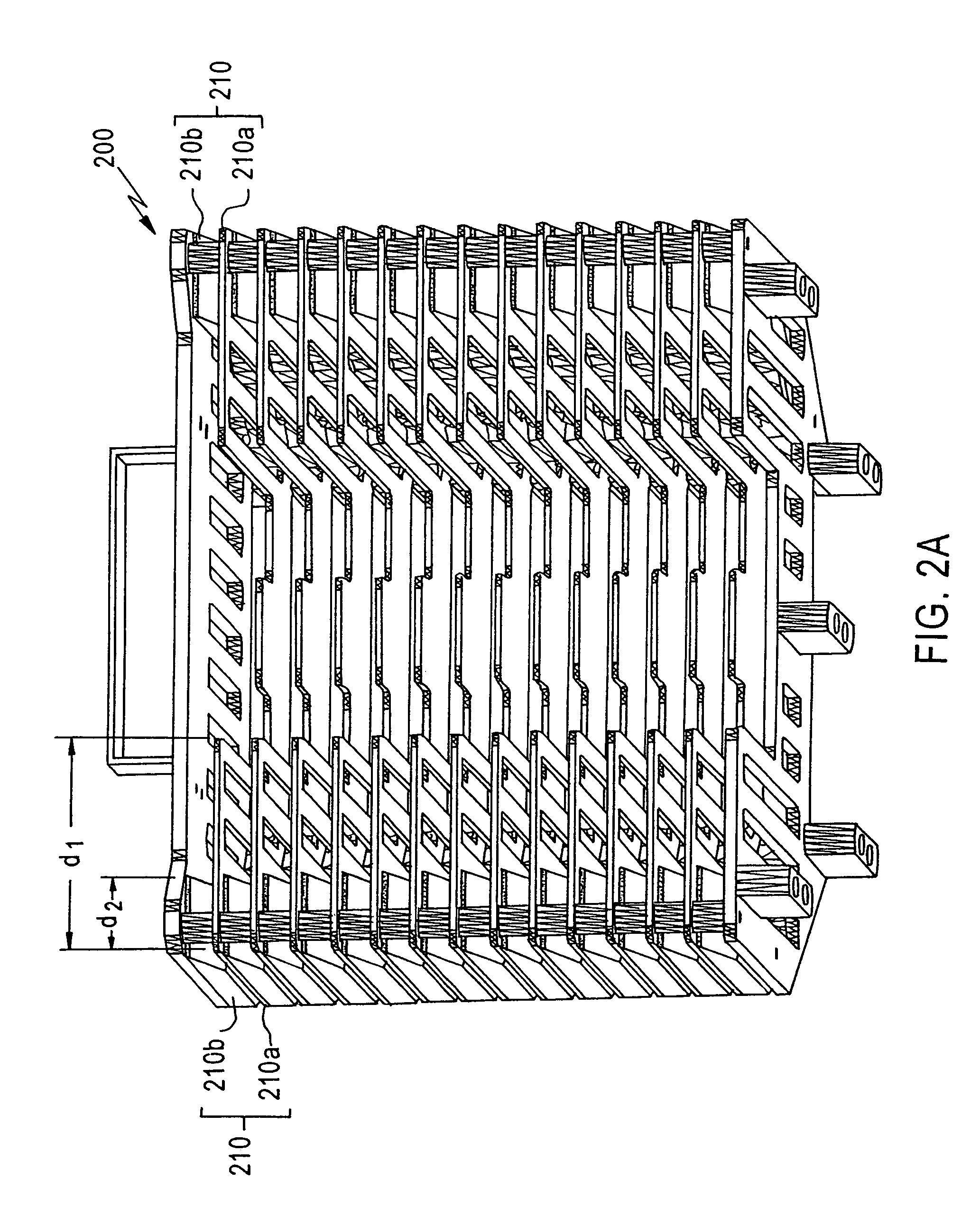
[0020]According to the present invention, a cassette for holding thin semiconductor wafers has a center support and a pair of edge supports for supporting the wafer in a predetermined reference plane, so that tools such as robots or automatic handlers can be programmed to pick them up without damaging them. As used throughout the present disclosure and claims, the term “wafer” denotes a semiconductor wafer, such as a silicon wafer. The inventive cassettes each have a plurality of sets of center and edge supports, the sets being spaced from each other a distance greater th...


PUM

PropertyMeasurementUnit
thicknessaaaaaaaaaa
thicknessaaaaaaaaaa
thicknessaaaaaaaaaa

Abstract

Cassettes for holding thin semiconductor wafers for safe handling are provided, along with an improved methodology for reducing the thickness of semiconductor wafers. Embodiments include a cassette for holding thin semiconductor wafers, having a plurality of sets of center and edge supports, the sets being spaced from each other a distance greater than a sag amount of the wafers. The thin wafers are supported in a predetermined reference plane, so that tools such as robots or automatic handlers can be programmed to pick them up without damaging them. In another embodiment, a double into single pitch wafer cassette is provided having a wafer entrance section with spacing twice as large between sets of edge supports as a conventional cassette, to accommodate the sag/warp of the thin wafers, and a “flattening section” which guides and flattens the wafers between opposing edge supports as they are pushed into the cassette, such that the wafers are held substantially planar. Because the wafers are held substantially planar, they can be safely removed from the cassette by automatic tools. A methodology is also provided for reducing the thickness of a semiconductor wafer, comprising grinding the back side of the wafer to reduce its initial thickness to an intermediate thickness, and plasma etching the back side of the wafer to reduce the intermediate thickness to a final thickness. The two-step grinding/etching process is faster and less expensive than conventional multi-step grinding/polishing processes, because it requires less steps, each step is accomplished relatively quickly, and it employs standard grinding and etching equipment, rather than expensive dedicated equipment.

Description

RELATED APPLICATION[0001]This application is a Divisional of U.S. patent application Ser. No. 10 / 460,164, filed Jun. 13, 2003, now abandoned.FIELD OF THE INVENTION[0002]The present invention relates to the handling of semiconductor wafers for making semiconductor devices. The present invention has particular applicability in handling thin wafers which are not rigid.BACKGROUND ART[0003]Conventional techniques for handling semiconductor wafers (such as silicon wafers) during processing, and in particular for transferring wafers between processing tools, typically involve standard-sized cassettes which hold a plurality of wafers at a time; e.g., about 14 wafers to a cassette. The wafers are typically supported by their edges by “fins” protruding inward from the sides of the cassettes. Handling chucks or “forks” associated with robotic and / or automatic equipment are used to remove wafers from the cassettes one at a time by supporting the wafer from the bottom, inboard of the cassette fi...

Claims


Application Information

Patent Timeline
Patent Type & Authority Patents(United States)
IPC IPC(8): H01L21/302
CPCH01L21/02008H01L21/6732H01L21/3065Y10T29/41
Inventor FOONG, SALLY Y. L.SEE-KEE, LIMNAM, WONG KWET
Owner ADVANCED MICRO DEVICES INC
Why Eureka
Try Eureka