Method to produce a factory programmable IC using standard IC wafers and the structure

a technology of ic wafers and factory programmable ic, which is applied in the direction of basic electric elements, electrical apparatus, semiconductor devices, etc., can solve the problems of not including non-volatile memory, not conducive to storing permanent device configuration data, and large user flexibility, so as to reduce the thickness of the wafer, reduce the difference in thermal conductivity between metal and silicon or silicon dioxide, and minimize heat flow

Inactive Publication Date: 2005-03-08
XILINX INC
View PDF8 Cites 8 Cited by
  • Summary
  • Abstract
  • Description
  • Claims
  • Application Information

AI Technical Summary

Benefits of technology

Because of the reduced thickness of the wafer, thermal conduction away from the immediate vicinity of the heated gate (and source / drain for salicide or base / emitter / collector for bipolar) is minimized. The difference in thermal conductivity between metal and silicon or silicon dioxide is small. The thinning is to minimize heat flow into the bulk of the wafer. In addition, it keeps the heat localized so it doesn't affect nearby transistors. The resulting concentrated heating causes diffusion of the dopant atoms in the source (emitter), drain (collector), and channel (base) regions of the element. Eventually, the source (emitter) and drain (collector) regions of the element merge, placing the element in a permanently “on” (i.e. programmed) configuration. An additional benefit of this methodology is that no visible indication of programming is created, enhancing the security of the programmed data.
The support structure can comprise any material capable of providing structural reinforcement of the semiconductor structure during and after the thinning operation, such as an unprocessed wafer, a processed wafer, or even a plastic or metal plate. Likewise, any mounting method can be used to attach the support structure to the top surface of the wafer, so long as the mounting method does not damage the elements formed on the wafer. Such methods can include the use of epoxy adhesives or covalent bonding. The thinning operation itself can be performed using any backside thinning technique, including grinding, chemical-mechanical polishing (CMP), and etching. The final thickness of the processed wafer is selected to minimize heat transfer away from the immediate vicinity of the element during programming, without overly degrading the structural integrity of the wafer or damaging the elements formed on the wafer surface.
As noted previously, the support structure is intended to reinforce the wafer during and after the thinning operation. Such reinforcement will typically be required for a bulk thinning process, such as grinding, CMP, or non-masked etch. Such bulk processes can reduce the thickness of the entire substrate, thereby substantially weakening the wafer and creating a need for supplementary reinforcement. However, according to another embodiment of the present invention, a localized etch process thins the wafer backside only at the locations of interest for programming purposes (i.e. under the transistors being made available for programming). By removing material from only a small portion of the wafer, the need for structural reinforcement is eliminated. A laser can then be used to program the desired elements as described previously, with the local thickness reductions minimizing heat transfer away from the source, drain, and channel regions during programming.

Problems solved by technology

However, many ICs do not include non-volatile memory in which such permanent configurations could be stored.
For example, high-density field programmable gate arrays (FPGAs) are typically produced using static random access memory (SRAM) technology, which provides a large degree of user flexibility but is not conducive to storing permanent device configuration data.

Method used


Image

  • Method to produce a factory programmable IC using standard IC wafers and the structure
  • Method to produce a factory programmable IC using standard IC wafers and the structure
  • Method to produce a factory programmable IC using standard IC wafers and the structure

Examples


Embodiment Construction

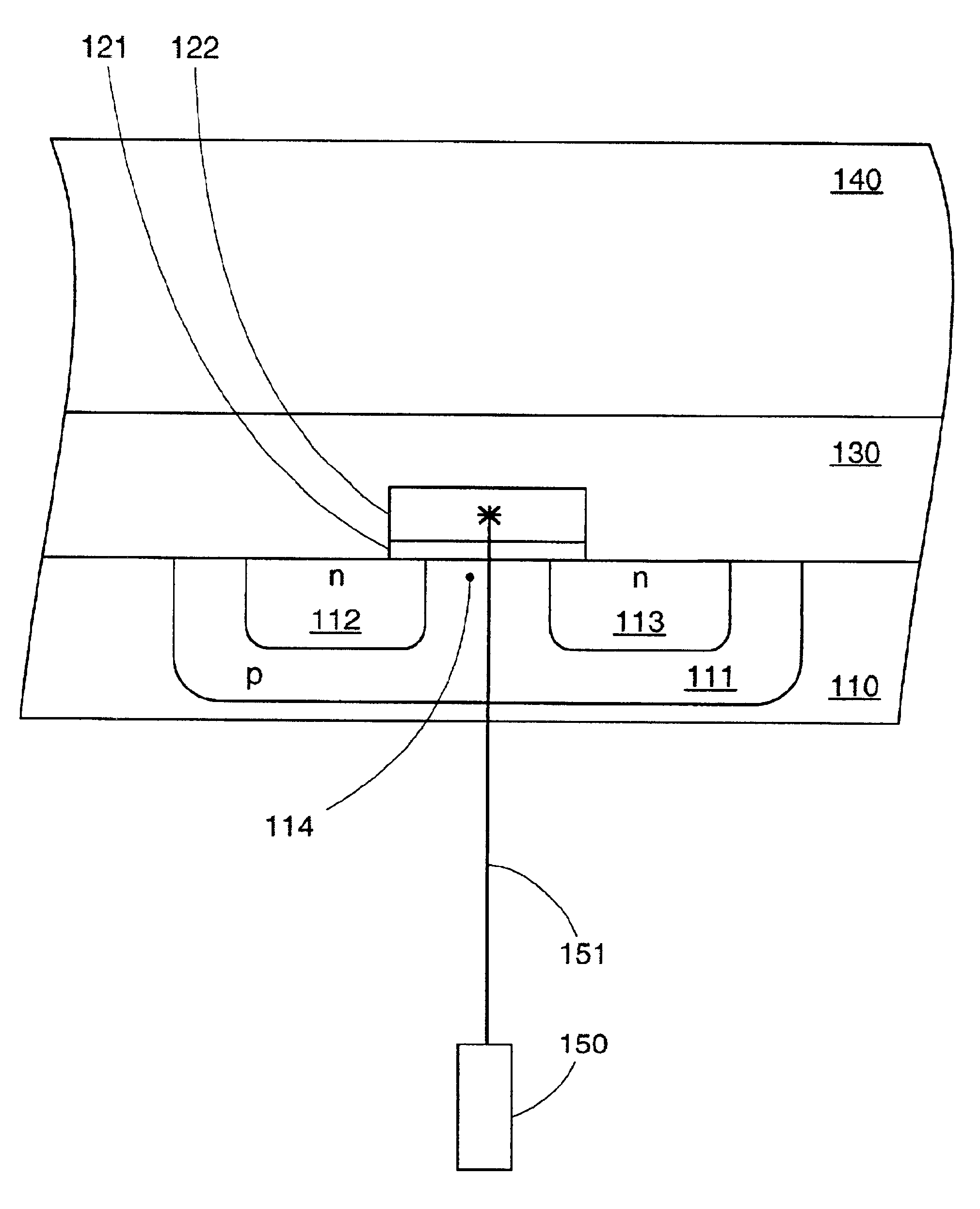
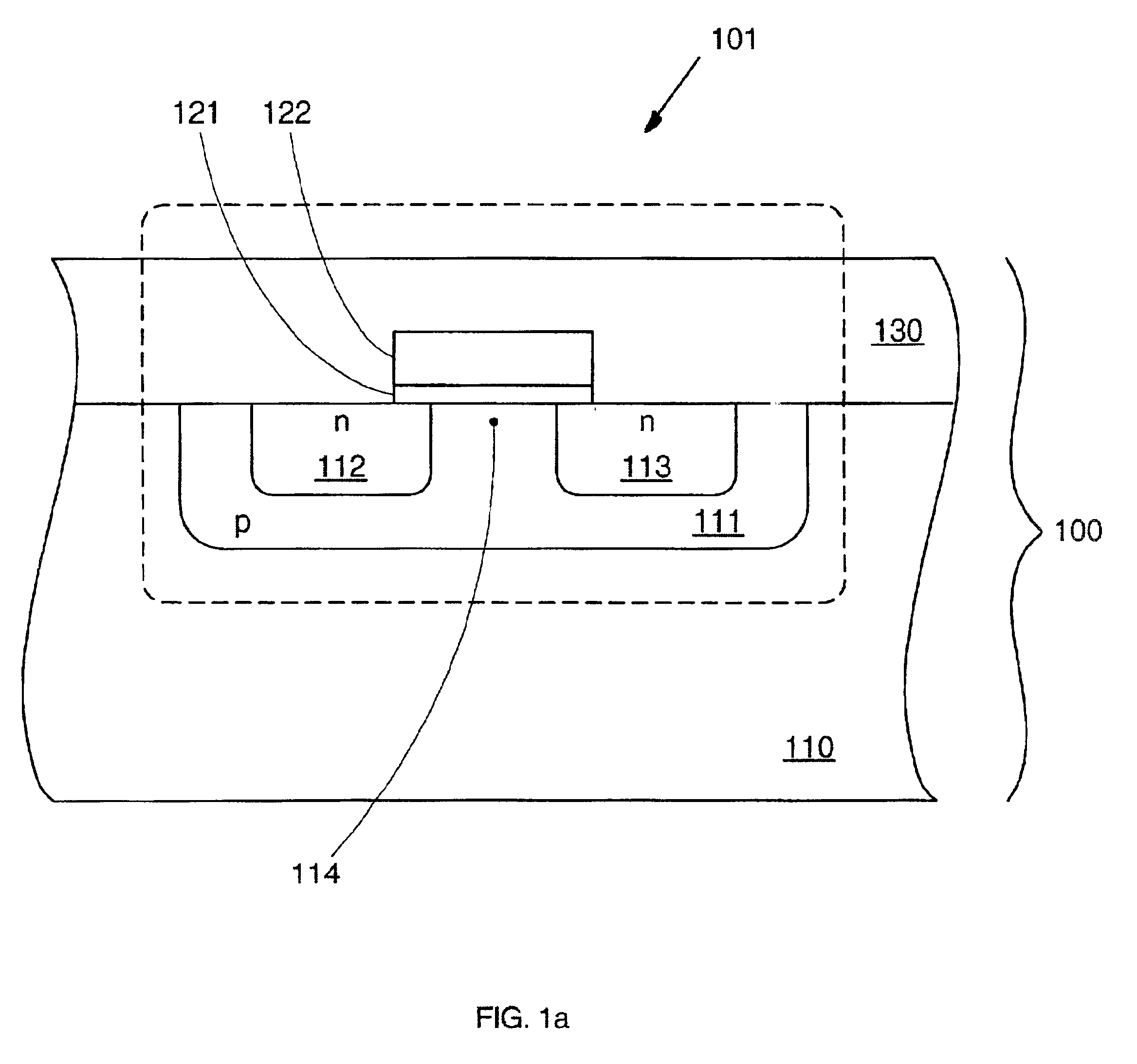
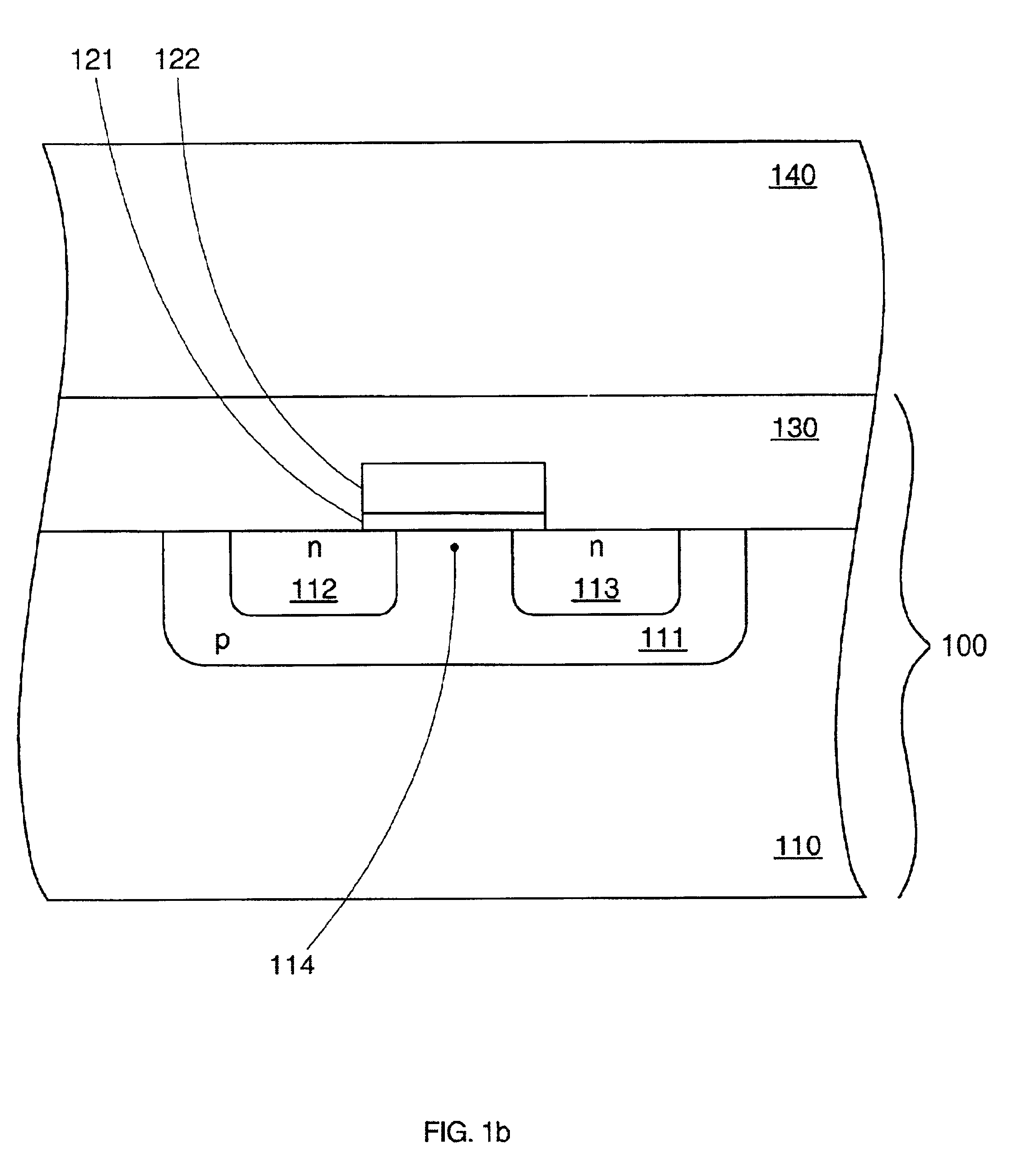
FIG. 1a shows a semiconductor element 101 formed as part of a processed semiconductor structure 100. Processed semiconductor structure 100 can comprise any type of semiconductor structure (e.g., FPGA wafers, memory wafers, etc.) formed using any type of semiconductor process (e.g., MOSFET, bipolar, etc.) and semiconductor technology (e.g., silicon, gallium arsenide, etc.).

Semiconductor element 101 comprises a metal-oxide-semiconductor (MOS) transistor located in a p-well 111 formed in a semiconductor substrate 110. Semiconductor substrate, 110 can comprise any support structure on which semiconductor elements can be formed, such as a silicon wafer, a glass or other insulating plate, or even a multi-layer structure such as an amorphous silicon layer formed on a metal sheet. Semiconductor element 101 comprises an n-type source 112 and an n-type drain 113, which are formed in p-well 111 and define a channel region 114. Semiconductor element 101 further comprises a gate oxide 121 over c...


PUM


Abstract

A method for programming a semiconductor element in a semiconductor structure such as an IC involves reducing the backside thickness of the substrate and directing an energy beam through the backside at an opaque component of the semiconductor element. A support structure mounted on the semiconductor structure provides support during and after the thinning operation. Alternatively, the substrate can be thinned only under the semiconductor element, leaving the rest of the substrate thick enough to maintain structural integrity. The energy beam heats the opaque component. The prior thinning operation minimizes heat dissipation away from the semiconductor element, so that dopant diffusion occurs, changing the electrical characteristics of the semiconductor element. By modifying selected elements in this manner, a semiconductor structure can be permanently programmed, even if it does not include non-volatile memory. Additionally, security is enhanced since the programming leaves no visible signs.

Description

FIELD OF THE INVENTIONThe present invention relates to integrated circuits, and in particular to a method for permanently modifying transistors using a laser.BACKGROUND OF THE INVENTIONIt is often desirable to be able to factory program integrated circuits (ICs), i.e. introduce permanent changes into the ICs at the fab, for example, to create an ID tag or provide an encryption key. However, many ICs do not include non-volatile memory in which such permanent configurations could be stored. For example, high-density field programmable gate arrays (FPGAs) are typically produced using static random access memory (SRAM) technology, which provides a large degree of user flexibility but is not conducive to storing permanent device configuration data. And even when non-volatile memory is available, it can be useful to have available alternative means of programming that do not consume those non-volatile memory resources. Accordingly, it is desirable to provide a method for factory programmi...

Claims


Application Information

Patent Timeline
Patent Type & Authority Patents(United States)
IPC IPC(8): H01L21/70H01L21/02H01L27/112H01L21/268H01L21/8246
CPCH01L21/268H01L27/1126H01L27/112H10B20/383H10B20/00
Inventor CONN, ROBERT O.
Owner XILINX INC
Why Eureka
Try Eureka