Solid state charge qubit device

a qubit device and solid state technology, applied in semiconductor devices, instruments, computing, etc., can solve the problems of increasing the number of qubits, and achieve the effects of reducing the number of qubits, and facilitating the performance of nanofabrication

Active Publication Date: 2006-07-13
NEWSOUTH INNOVATIONS PTY LTD
View PDF1 Cites 54 Cited by
  • Summary
  • Abstract
  • Description
  • Claims
  • Application Information

AI Technical Summary

Benefits of technology

[0026] The entire device may be cooled well-below room temperature to ensure that the donors are not thermally ionised and to minimise coupling of the charge qubits to the environment. More specifically it may be cooled to liquid helium temperatures of 4K or below.
[0031] Furthermore, since the Coulomb interaction acts over a longer range than spin-spin interactions, the charge qubit devices can be made larger than their spin-based counterparts. In particular, P donors in the Kane architecture are ideally placed 20 nm apart, while the donor separation for charge qubits could be as large as 200 nm with the appropriate choice of substrate and gate potentials. This increased scale makes nanofabrication considerably easier.
[0032] Given that the fabrication process is very similar, the main advantage of the real-spin over the charge qubit is the long decoherence times. However, the trade-off is in the measurement process: measurement of the charge state qubit is considerably easier to perform than the single-spin measurement scheme as envisaged by Kane.

Problems solved by technology

Since a system of qubits can never be totally isolated from the environment, error-correcting schemes must be incorporated in the design and encoding of the qubits, further increasing the number of qubits required.
The real challenge is to prove the principle of QC in a technology which is inherently scalable.

Method used


Image

  • Solid state charge qubit device
  • Solid state charge qubit device
  • Solid state charge qubit device

Examples


Embodiment Construction

The P—P+ Charge Qubit

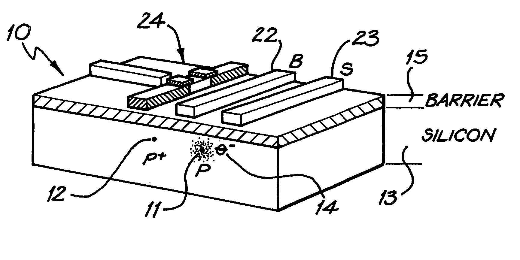
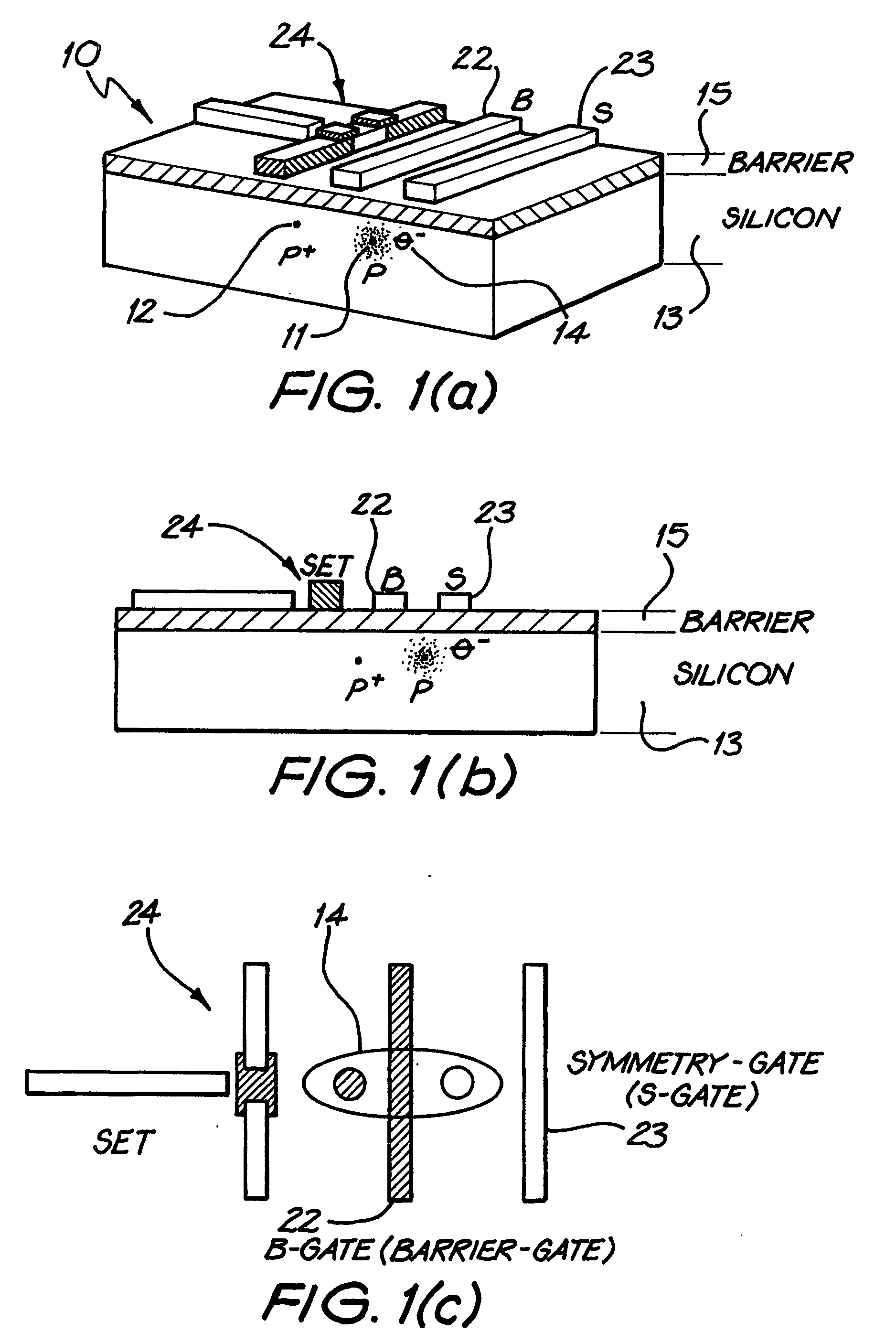
[0086] Referring first to FIGS. 1 and 2, a charge qubit 10 is based on electrons localized by two donor P atoms 11 and 12 buried in a silicon substrate 13. Each qubit comprises an “artificial molecule” P—P+ system in which a single electron 14 remains. The other donor electron must previously be removed from the system by an ionization process, such as electric field induced ionization produced by suitable gate biaising. Gates placed above the buried P—P+ system, on a non-conducting barrier layer 15 allow for external control.

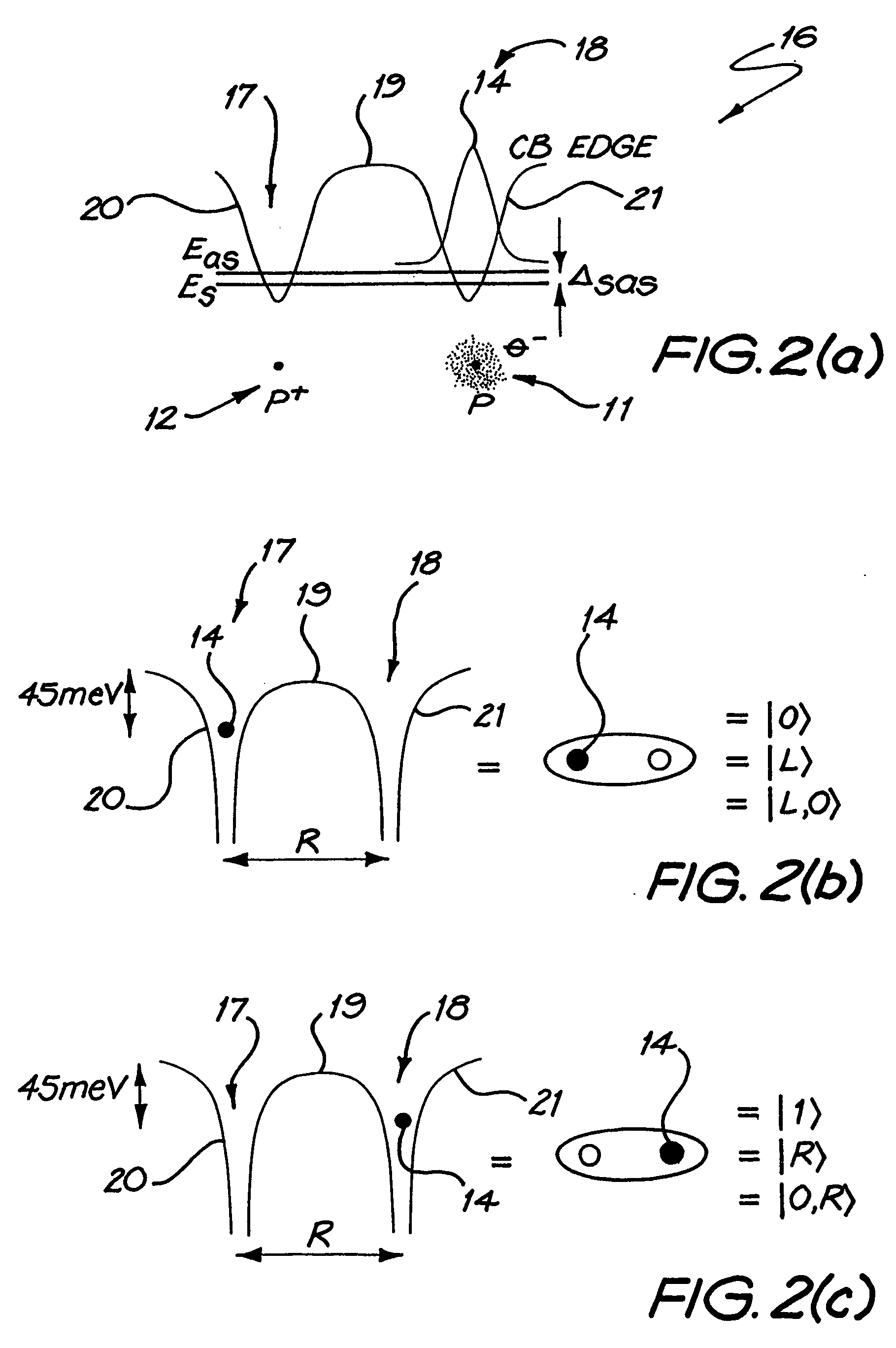
[0087] The remaining electron 14 exists in a double-well potential 16, in one or other of the wells. In the potential diagrams the double-well potential 16 has a left-hand well 17 and a right hand well 18. Between the wells is a potential barrier 19, and there are potential barriers 20 and 21 outside the wells. A basic qubit and definition of logical states in terms of left 17 and right 18 localized states with respect to the double-well...


PUM


Abstract

Ionisation of one of a pair of dopant atoms (11, 12) in a substrate (13) creates a double well potential, and a charge qubit is realised by the location of one or more electrons or holes (14) within this potential. The dopant atoms may comprise phosphorous atoms, located in a silicon substrate. A solid state quantum computer may be formed using a plurality of pairs of dopant atoms (11, 12), corresponding gate electrodes (22, 23), and read-out devices comprising single electron transistors (24).

Description

TECHNICAL FIELD [0001] This invention concerns a quantum device, suitable for quantum computing, based on dopant atoms located in a solid semiconductor or insulator substrate. In further aspects the device is scaled up. The invention also concerns methods of reading out from the devices, initializing them, using them to perform logic operations and making them. BACKGROUND ART [0002] There are a number of existing proposals for quantum computing (QC) based on charge qubits in the solid-state. There is also the Kane proposal for a real spin quantum device based upon phosphorus donor atoms in silicon. Proposals relevant to this invention are now presented in chronological order: [0003] Logical devices implemented using quantum cellular automata, P. D. Tougaw and C. S. Lent, J. Appl. Phys. 75, 1818 (1994). [0004] Conditional quantum dynamics and logic gates, A. Barenco, D. Deutsch, Ekert and Josza, Phys. Rev. Lett. 74, 4083 (1995). [0005] Minimal energy requirements in communication, R....

Claims


Application Information

Patent Timeline
Patent Type & Authority Applications(United States)
IPC IPC(8): H01L31/109G06N99/00
CPCB82Y10/00G06N99/002Y10S977/933G06N10/00
Inventor HOLLENBERG, LLOYD CHRISTOPHER LEONARDDZURAK, ANDREW STEVENWELLARD, CAMERONHAMILTON, ALEXANDER RUDOLFREILLY, DAVID J.MILBURN, GERARD J.CLARK, ROBERT GRAHAM
Owner NEWSOUTH INNOVATIONS PTY LTD
Why Eureka
Try Eureka