In situ doped embedded sige extension and source/drain for enhanced pfet performance

a technology of embedded sige and source/drain, which is applied in the direction of basic electric elements, electrical equipment, semiconductor devices, etc., can solve the problems of cmos transistor carrier mobility being difficult to enhance, and the silicon channel affecting the mobility of cmos transistor carriers is significant, so as to prevent growth on the gate

Active Publication Date: 2006-07-13
MICROSOFT TECH LICENSING LLC
View PDF8 Cites 22 Cited by
  • Summary
  • Abstract
  • Description
  • Claims
  • Application Information

AI Technical Summary

Benefits of technology

[0006] Then, the invention epitaxially grows strained silicon germanium in the openings. A portion of the substrate below the gate stacks of the P-type transistors comprises a channel region and the strained silicon germanium creates longitudinal stress on the channel region. The process of epitaxially growing the strained silicon germanium is a selective epitaxy process and can be in-situ doped with boron. The invention uses protective caps over the gate stacks of the P-type transistors to protect gates of the P-type transistors during the process of removing the upper portions of the P-type transistors extension and source / drain regions and prevent growth on the gates during subsequent SiGe epitaxy process.

Problems solved by technology

It has been shown that the strain in the silicon channel can affect the mobility of CMOS transistor carriers significantly.
Hole mobility is more difficult to enhance in this approach since a very large Ge percentage is required.

Method used


Image

  • In situ doped embedded sige extension and source/drain for enhanced pfet performance
  • In situ doped embedded sige extension and source/drain for enhanced pfet performance
  • In situ doped embedded sige extension and source/drain for enhanced pfet performance

Examples


Embodiment Construction

[0018] The present invention and the various features and advantageous details thereof are explained more fully with reference to the nonlimiting embodiments that are illustrated in the accompanying drawings and detailed in the following description. It should be noted that the features illustrated in the drawings are not necessarily drawn to scale. Descriptions of well-known components and processing techniques are omitted so as to not unnecessarily obscure the present invention. The examples used herein are intended merely to facilitate an understanding of ways in which the invention may be practiced and to further enable those of skill in the art to practice the invention. Accordingly, the examples should not be construed as limiting the scope of the invention.

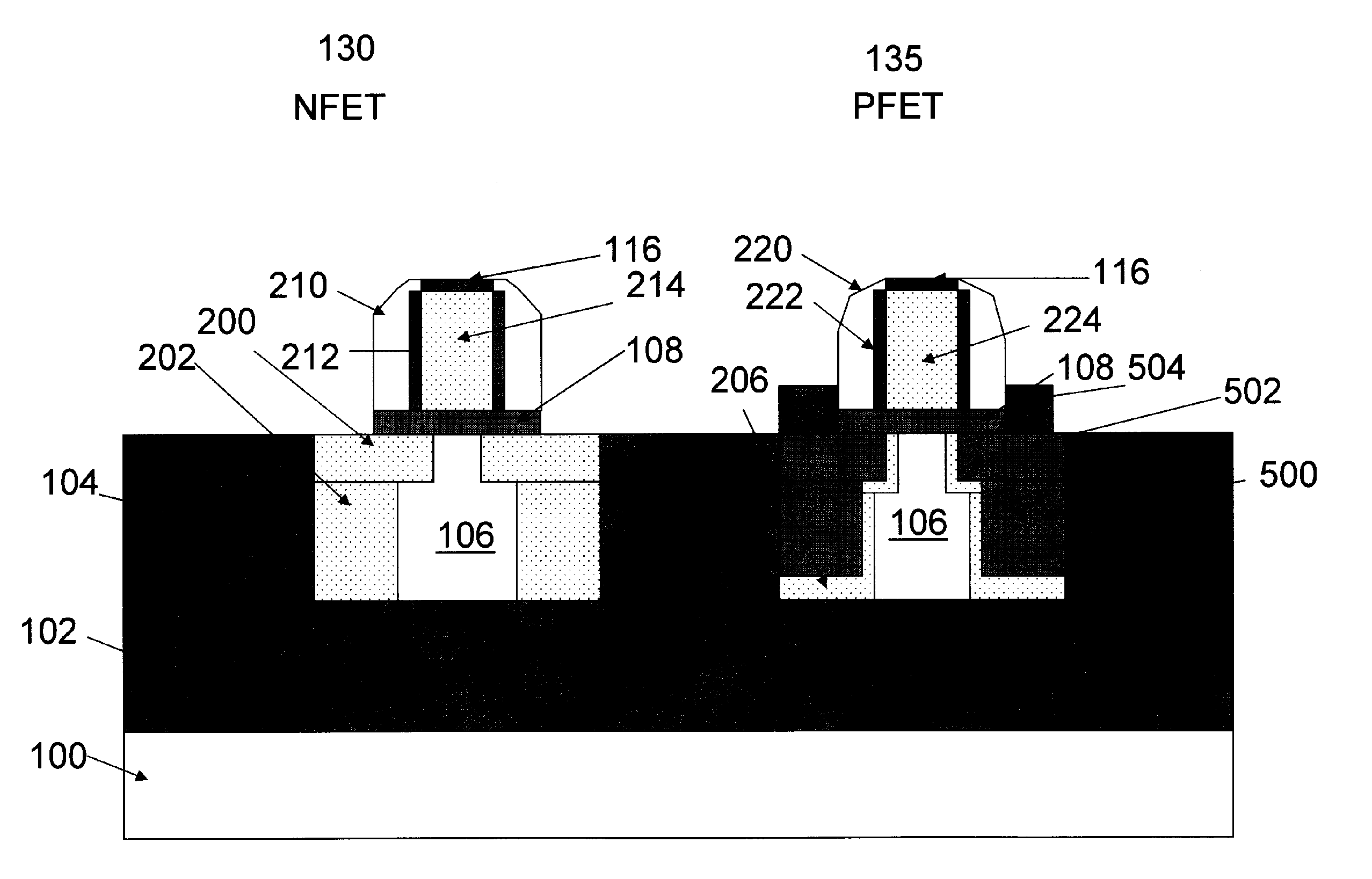
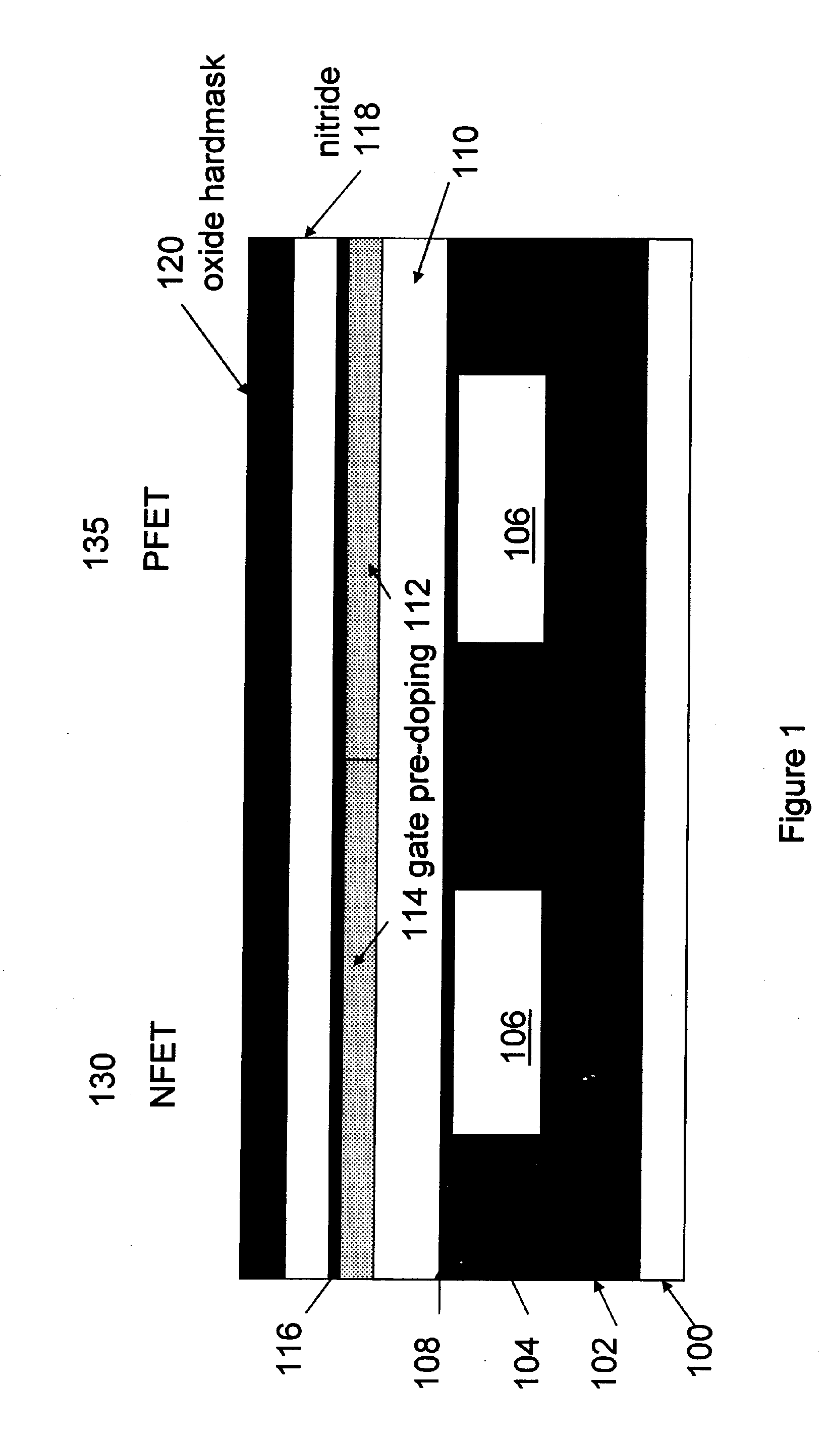
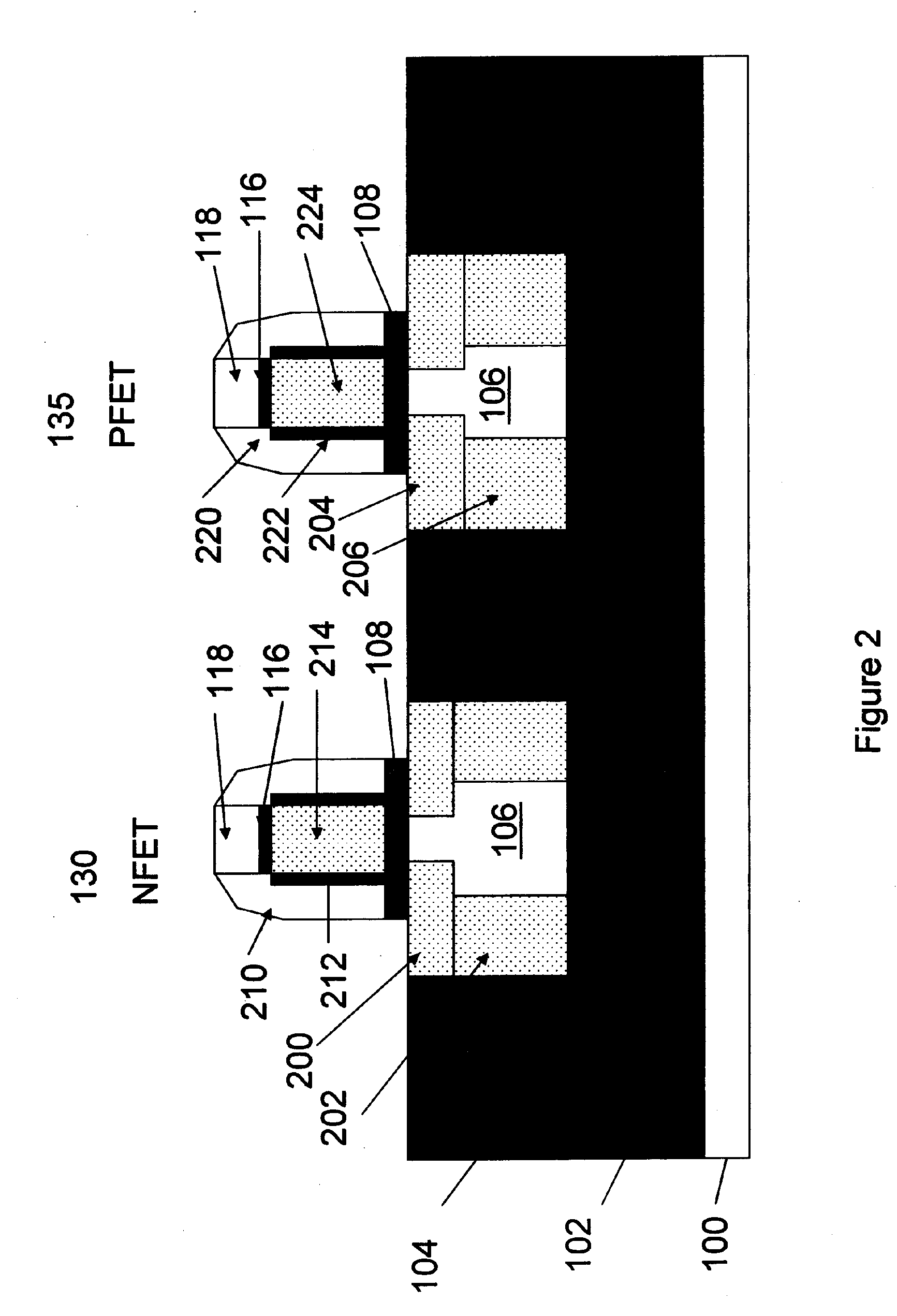
[0019] Referring now to the drawings, FIG. 1-7 illustrate one embodiment of the invention. In FIG. 1, item 100 represents a silicon substrate, and item 102 represents a buried oxide (BOX). Layer 104 is a silicon on insulat...


PUM


Abstract

Disclosed is an integrated circuit structure and a method of making such a structure that has a substrate and P-type and N-type transistors on the substrate. The N-type transistor extension and source / drain regions comprise dopants implanted into the substrate. The P-type transistor extension and source / drain regions partially include a strained epitaxial silicon germanium, wherein the strained silicon germanium comprises of two layers, with a top layer that is closer to the gate stack than the bottom layer. The strained silicon germanium is in-situ doped and creates longitudinal stress on the channel region.

Description

FIELD OF THE INVENTION [0001] The invention generally relates to an integrated circuit structure that has P type and N type transistors where strained silicon germanium in the P type extension and source / drain regions creates longitudinal stress on the channel region of the P type transistors. DESCRIPTION OF THE RELATED ART [0002] U.S. Pat. No. 6,621,131 to Murthy (hereinafter “Murthy”) discloses embodiments that were satisfactory for the purposes for which they were intended. The disclosure of Murthy, in its entirety, is hereby expressly incorporated by reference into the present invention for purposes including, but not limited to, indicating the background of the present invention and illustrating the state of the art. It has been shown that the strain in the silicon channel can affect the mobility of CMOS transistor carriers significantly. Compressive longitudinal stress along the channel is known to help the PFET (P-type field effect transistor) drive current while it degrades ...

Claims


Application Information

Patent Timeline
Patent Type & Authority Applications(United States)
IPC IPC(8): H01L29/94
CPCH01L21/823807H01L21/823814H01L29/7842H01L29/7848
Inventor CHEN, HUAJIECHIDAMBARRAO, DURESETIPANDA, SIDDHARTHAOH, SANG-HYUNUTOMO, HENRY K.RAUSCH, WERNER A.
Owner MICROSOFT TECH LICENSING LLC
Why Eureka
Try Eureka