Noncontact conductivity measuring instrument

a conductivity measurement and non-contact technology, applied in the direction of instruments, individual semiconductor device testing, resistance/reactance/impedence, etc., can solve the problems of large and expensive network analyzers, inability to dedicate sample measurement with microwaves, and difficulty in using network analyzers as industrial instruments, etc., to achieve simple and compact configuration

Inactive Publication Date: 2006-07-13
TOHOKU TECHNO ARCH CO LTD
View PDF5 Cites 9 Cited by
  • Summary
  • Abstract
  • Description
  • Claims
  • Application Information

AI Technical Summary

Benefits of technology

[0010] According to the above configuration, a noncontact conductivity measuring instrumen

Problems solved by technology

However, currently there is no instrument dedicated to the sample measurement with the microwave, and a network analyzer which measures an S parameter of a passive and active network of an electronic in

Method used


Image

  • Noncontact conductivity measuring instrument
  • Noncontact conductivity measuring instrument
  • Noncontact conductivity measuring instrument

Examples


embodiment

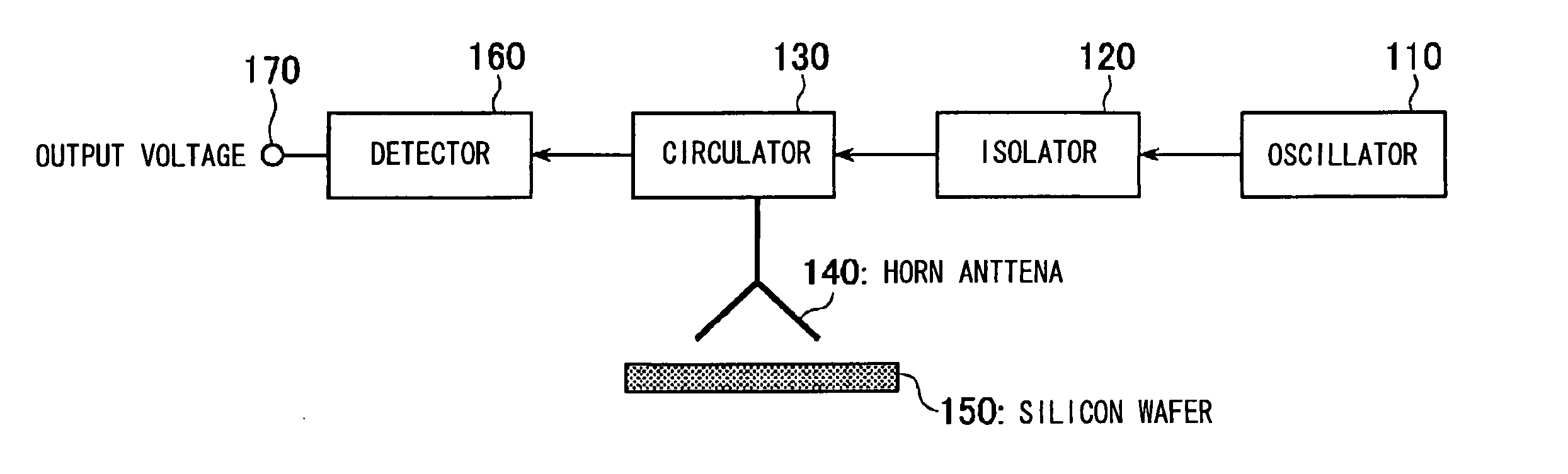
[0026] In the configuration of the measuring instrument with the microwave, actually the silicon wafer was used to measure the conductivity.

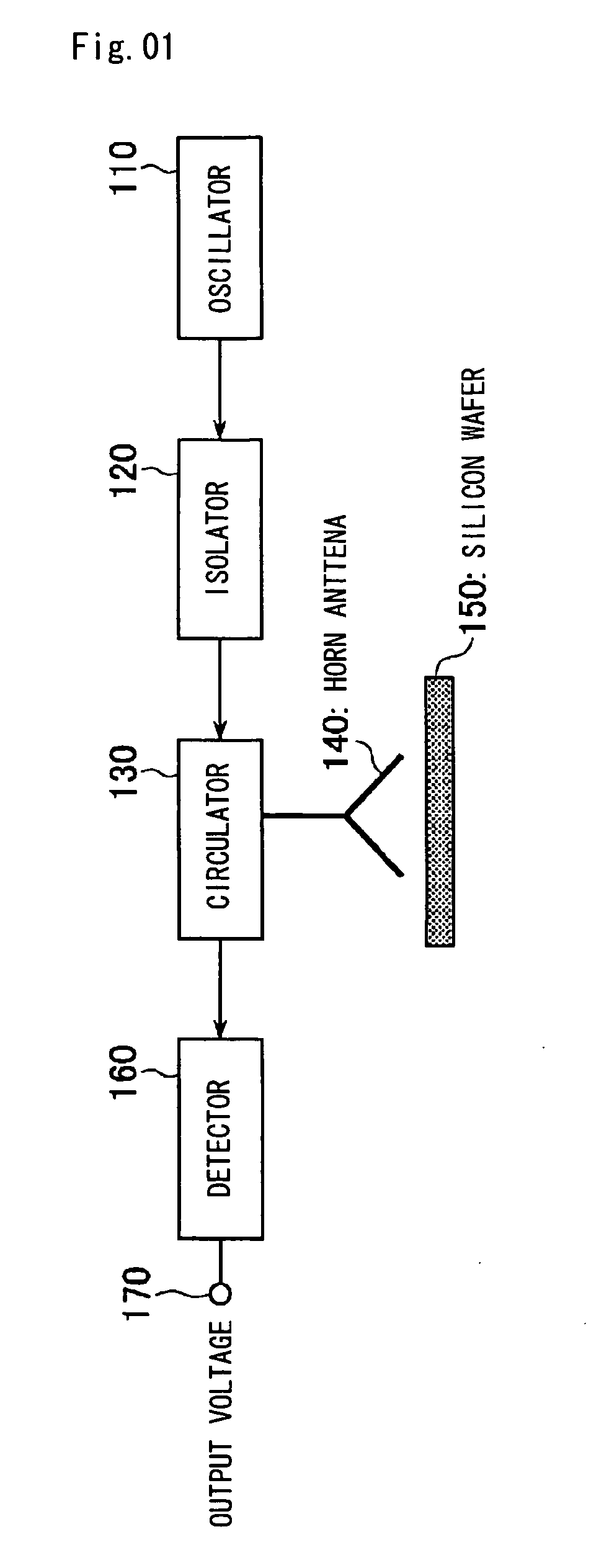
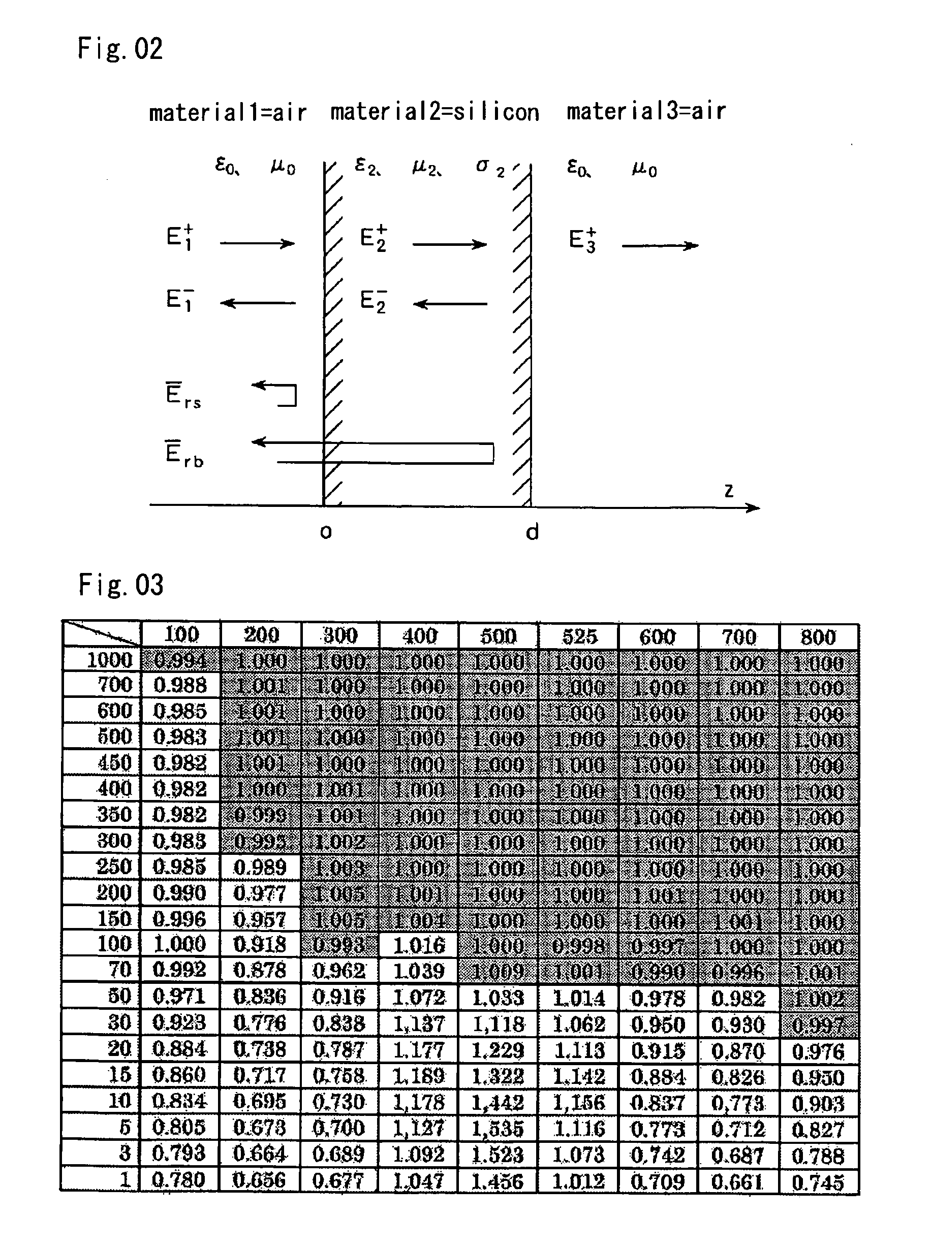
[0027] Seven n-type silicon wafers S1 to S7 were prepared as a specimen. In the silicon wafers S1 to S7, a diameter was 100 mm, the thickness was 525±≅μm, and P was doped. The silicon wafer used in the measurement was formed by a cz method, and mirror polishing was performed to the surface used in the measurement. The silicon wafer conductivity a measured by the four-probe method ranged from 58 to 212 S / m. A copper plate, in which the conductivity was 2.8×10⁷ S / m and the dimensions were 50×50×2 mm, was also prepared. It is assumed that the absolute values and the output voltages of the reflectance of the silicon wafers S1 to S7 are set at |Γk| and vk (k=1 to 7) respectively and the reflectance and the output voltage of the copper plate are set at |Γcu| and vcu respectively. At this point, because it is thought that the total reflection of the m...


PUM


Abstract

The present invention relates to measurement of conductivity, particularly to the noncontact measurement of the conductivity using a microwave. A microwave oscillated by an oscillator (110) using a Gunn diode is applied through an isolator (120), a circulator (130), and a horn antenna (140) to a silicon wafer (150). The isolator (120) is used for reducing the standing wave influencing the operation of the instrument. The reflected wave is received by the same horn antenna (140), detected by a detector (160) connected to the circulator (130), and outputted in the form of a voltage. The detector (160) produces an output voltage proportional to the square of the amplitude of an electric field. Since the amplitude of the reflected wave from a silicon wafer (150) is proportional to the absolute value of the reflectance, the output voltage is also proportional to the square of the absolute value of the reflectance. The reflectance is in a certain relationship with the conductivity, the conductivity of the silicon wafer (150) can be determined.

Description

TECHNICAL FIELD [0001] The present invention relates to measurement of conductivity, particularly to the noncontact measurement of the conductivity using a microwave. BACKGROUND ART [0002] The measuring method with the microwave is adopted in the noncontact conductivity measurement of a silicon wafer (see Non-Patent Reference 1 and Patent Reference 1). The noncontact measurement can be realized by using the microwave which can propagate through air. The microwave has an advantage that reaction of the microwave is directly associated with electric properties of a sample. [0003] However, currently there is no instrument dedicated to the sample measurement with the microwave, and a network analyzer which measures an S parameter of a passive and active network of an electronic instrument is usually used as an alternative to the dedicated instrument. Because the network analyzer is large and expensive, it is difficult that the network analyzer is used as an industrial instrument. [0004] ...

Claims


Application Information

Patent Timeline
IPC IPC(8): G01R27/04G01N22/00G01R31/26
CPCG01R27/04G01R31/2648
Inventor JU, YANG
Owner TOHOKU TECHNO ARCH CO LTD
Why Eureka
Try Eureka